IBIS-AMI: Modeling architecture study

Preface:

In previous post, we discussed several possible roles involving IBIS-AMI and their points of considerations. In this post, we would like to focus on the AMI model developer’s role and explore several modeling flows along with their pros and cons. The materials and example discussed here are from publicly available sources and articles, which are also listed at the end of this post.

IBIS-AMI models:

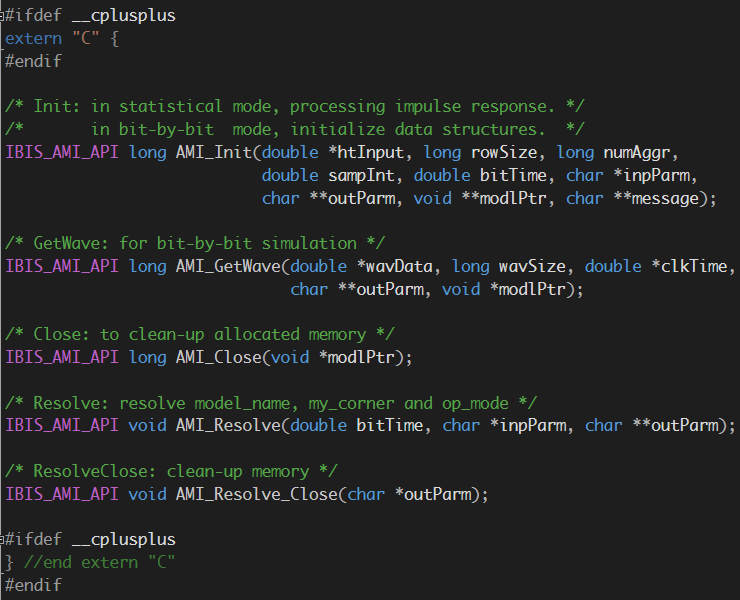
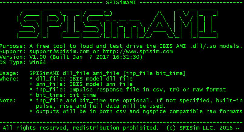
Regardless how sophisticated a SERDES design is, at the end of the day, the work of generating a corresponding AMI model is to create the following the 3 ~ 5 (depending on IBIS spec. version) AMI API functions in C language and compile them as .dll(s)/.so(s) across different platforms and OSes. Noted that the actual implementations (how the SERDES or EQ operates) are not bounded by C/C++ language. For example, one may use matlab, octave, perl or other language to implement the core function, only that they have to be wrapped with C AMI-API functions. Regardless, the main objectives are still the same: translate the design to corresponding codes. On top of that, one also needs to consider how to debug, maintain and extend the generated models for model users and future design revision.

IBIS-AMI API functions

A very popular, and relatively easy approach to achieve this goal is to use tool/program to generate codes directly from design collateral.

Top-down AMI modeling flow:

A typical design flow is usually top-down based: floor plan is made and functional blocks are defined. At first, only abstract level behaviors, budgets and/or spec. are given. Each designer or team then dives into the detailed implementation of these functional blocks and finally assemble them together for full design simulation or verification. Using this approach, a schematic is usually used for design entry and connect different block first, each block may have several hierarchies. Architecture codes/schematics are translated to C/C++ by machine.

User also usually can right click on each block to specify parameters for customization or exporting. When it’s done, an add-on module will translate this design to corresponding C/C++ format most of the time. So far as AMI API is concerned, a special AMI kit may be also needed such that generated codes will be AMI-API compatible.

With this approach, user focuses on SERDES design rather than the coding or API details. Since these architecture blocks/codes are pre-generated and verified, the generated codes are considered well tested and should produce good correlations.

Machine generated codes:

While machine/program generated codes are pre-tested and usually very structured, it may not be easy to debug and extend. While it’s certainly possible to rewrite part of the codes for fine tuning or customization, one should not forget that next time when the designer click “generated c/c++” button again, all the changes will be overwritten. So the update made at the bottom (i.e. generated codes) will not back propagate or back annotate to original design. One almost always have to change from the top.

My observations for this top-down approach are:

  • Suitable for designer who has original collateral, don’t know or want to code.
  • These are mostly machine generated codes:
    • Should run correctly as it has been tested
    • May not be efficient, (most of the case, certainly in this case above)
    • Not easy to maintain…. bad readability and can’t enforce coding guideline
    • One direction only, code changes can’t back propagate.

Bottom-up AMI modeling flow:

If a software developer is going to tackle the AMI modeling challenge, his/her approach probably will be different from that used by the SERDES/IC designer. If it’s me, a bottom-up approach will probably be used:

  • 1st, one will identify several common blocks to be used, such as
    • FFE: Feed-forward equalizer, LTI, Time or frequency domain
    • LPF: Low pass filter, LTI, freqeuncy domain
      • CTLE, Bassel, filter based IIR/FIR etc
    • DFE: Decision feedback equalizer, NLTV/digial, time domain only
    • CDR: Clock data recovery, NLTV/digital, time domain only
    • Coder: various coding page
      • 64b66b, 8b10b etc
    • PRBS: Pseudo random bit stream, PRBS7, 10, 15 etc
    • AFE: analog front end to convert pulse to shape with Rt/Ft/Swing etc
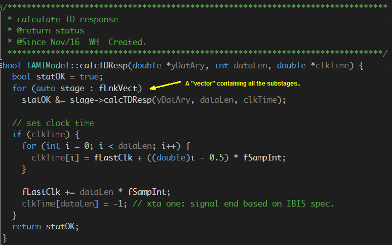
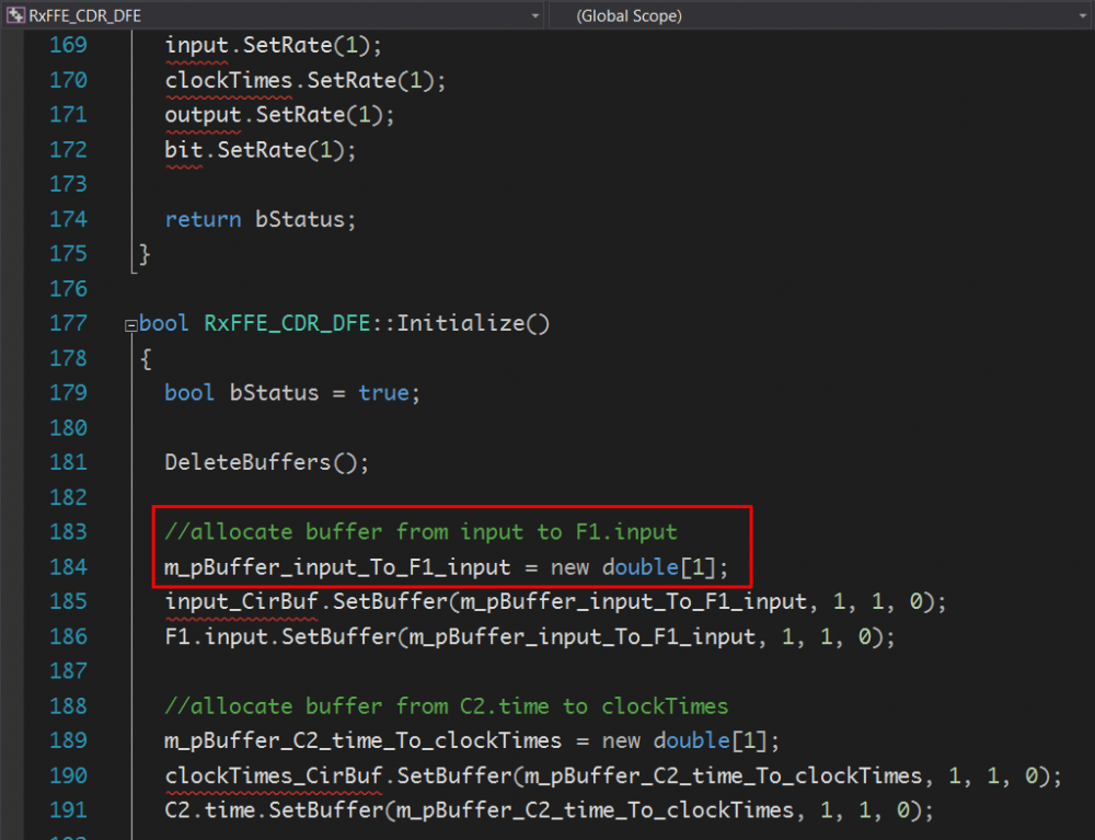
  • 2nd, one may define common interface, data member etc between these blocks and use OO principles to construct base and derived class etc

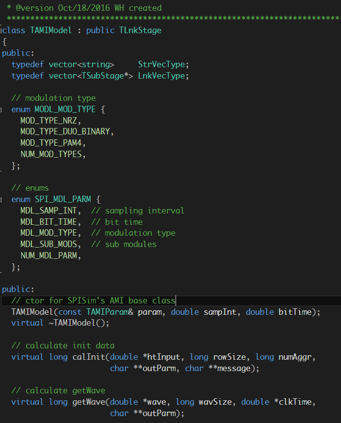
  • 3rd, being able to assemble different stages elegantly and form an AMI model of this stage:

  • As a bonus, one can then easily add extra mechanism such as security, encryption and/or different selector of different CTLE responses as an example.

Since this is hand cranked, the developer should feel very comfortable supporting, debugging and extending the functions. Accompanies with good documentation, it can be used for very long time. In order to make sure the model’s performance matches those from the original design:

  • The classes should not be hard coded with number. Instead, settings etc should be parameterized and can be tune either programmingly or from the .ami file
  • A “sweep”, least-squared-error based fit or other optimization methodology can be used to find the set of parameters which match the original design’s performance best
    • In other words, the good correlation is not “given”. It needs effort.

My observation of this bottom-up approach are:

  • Suitable for engineer person who is good at OO and comfortable coding:
  • Human written codes:
    • Need effort to make sure codes can run correctly
    • When doing it right, will run very efficiently
    • When doing it right, will be easy to maintain and extend
    • Code usability is very high, save effort/resources in the long run.

Spec/Datasheet based AMI modeling:

From the discussion above, it seems both top-down and bottom-up approaches each has its own merits. Is it possible to have best of both worlds?

It’s not easy… since each engineering’s disciplines are different, and that’s also why doing IBIS-AMI modeling is technical challenging. It demands cross-domain knowledge and experience at least. We haven’t even discussed algorithms such as FFT, iFFT, DSP, BER etc above yet…

Having that said, I believe that this still possible if we can eliminate short comings of either side. For example, One can look at other EDA vendors’ AMI library parts and find that they are actually well organized and architect like the bottom-up thinking above. So it must be the process which translates schematic to codes which compromised results. This is most likely due to its general purpose usage: “design anything and tool can translate to c/c++”.

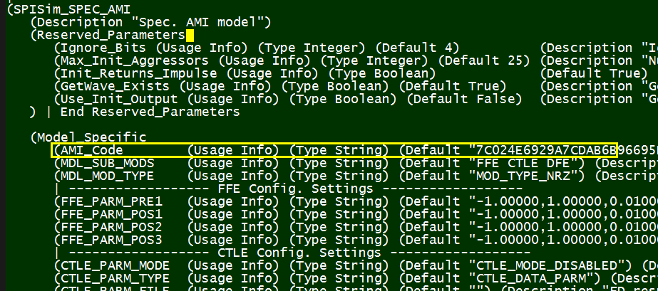
Since it’s not easy to change big EDA company’s product and application scope, if one can find suitable DSP/filter design library to use in the first place in the bottom-up flow, then a well behaved, efficient, maintainable and extensible modeling is not that out of reach. Fortunately, there are plenty of such open source libraries available. Further more, commonly used functional blocks can be assembled together based on settings or parameter. They can even be pre-built/pre-compiled so the compilation can be further avoided. The end result is template/spec/datasheet based, AMI modeling approach.

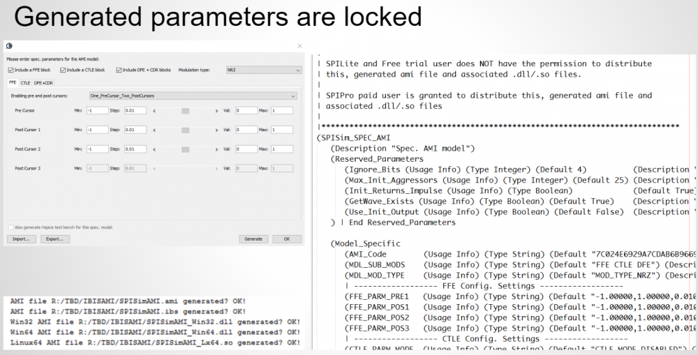
SPISimAMI: Spec/Datasheet based AMI modeling

Many recent publications, alone with the adoption of this approach from smaller EDA company like us, has supported this as a better modeling flow so far as IBIS-AMI is concerned.

Reference:

2015 DesignCon paper: [HERE]
2016 IBIS Summit paper: [HERE]
2016 DesignCon paper: [HERE]

IBIS-AMI: Scenerios

IBIS-AMI: roles and scenerios

SERDES based links, such as USB, PCIe and SATA, are now ubiquitous. Their SI analysis poses special challenges as low bit error rate required by their spec. means millions of bits needs to be simulated. In stead of using transistor level design details or proprietorial behavior blocks (e.g. Verilog-A or matalb model), an industrial standard, exchangeable modeling format are usually required. This is because Tx and Rx IPs may not be from the same vendors, nor are the simulator or analysis tools used by IC and system integrator. IBIS-AMI is currently the industrial standard for this purpose. Just like a traditional IBIS, only more cross-domain knowledge demanding and technical challenging. It requires certain flows to be able to test, generate, validate and release IBIS-AMI models. In addition, the considerations related to IBIS-AMI also depend on the these different roles and scenarios. We believe when developing or adopting AMI workflow, three usage situations, including 1. an end user, 2. a model developer and 3. a model publisher should all be considered thoroughly.

As an AMI model user:

This is the most common scenario. As a model user, one will often want to validate and test the received model first before running full simulation. Take an IBIS model as an example, the validation tasks usually include first: check with golden parser, then run time domain simulation driving IBIS model to simple test load and check response. More diligent users will also want to extract the performance matrices such as impedance and Rtt etc to make sure the it matches what’s claimed by the model name.

The example below show pretty good matches in terms of impedance of different corners (34 and 40 ohms).

When it comes to an AMI model, things are not that easy. First of all, AMI binary model files (.dll(s)/.so(s)) are not only OS (e.g. windows vs linux vs OSX) but also platform (e.g. 32 bit and 64 bit) dependent. This means that unless a model’s file name contain correct info (e.g. TX_Win32.dll), one usually can’t easily check by just looking into the content of the binary file. Secondly, depending on the version of the spec. the implemented APIs in the model are also different. Again, these implementations are in compiled format and one can’t easily check. Lastly, even the latest golden parser will not exercise these API calls, let alone checking their performance. And to excite an AMI model usually involve third party (often expensive) EDA tools usage and required license.

EDA tools like HSpice does provide a simple utility called AMICheck for this purpose. Similarly, companies like SiSoft and Cadence also provide some development kit which enable AMI model checking. However, in the HSpice’s case, a license is required to run this utility. For the later two cases, the development kit needs to be compiled into respective OS/paltform first and the input and output to the models are not flexible. All these poses obstacles which prevents a model user to be able to quickly check the received model.

We believe a simpler yet  more elegant solution should exist. That’s why we developed the SPISimAMI and release it as free tool. It’s also been compiled into different platform and can be freely download to use directly. With this utility, a user can drive given AMI dll file with accompanied .ami settings. Tool will first load the dll to make sure it matches the OS version of the executing SPISimAMI utility. It will then load the models and check mandatory API functions such as Ami_Init and Ami_Close. User can then use embedded rising/falling step and pulse response to drive these Ami_Init and Ami_GetWave functions if available (too will check whether the GetWave_exist is set to true). Alternatively, an user can pass the input response to the model in either .csv, .tr0 or .raw format. The output waveform from the model will then be saved as non-proprietorial .csv and .raw formats to be inspected by tool like excel or our free SPILite and SPIPro. The screenshot below show its usage:

An example of quick AMI check using this features is to feed input bit sequence and check the equalization level output from the AMI model:

Regardless which approach or tool one takes, we believe that as an AMI model user, these checking process and capabilities should be considered due diligence and must be done before performing full link analysis with these AMI models.

As an AMI model developer:

AMI model development usually requires cross domain expertise. For example, a model developer needs to know how AMI and associated IBIS models are used. Then computer science skills such as programming in C/C++, implement APIs and use compilers like Visual Studio and g++/gcc to produce .dll/.so are also required. Finally the domain knowledge such as DSP, equalization and link analysis come to play. In terms of implementation, a model developer not only needs to comprehend these technical details but also needs to architecture codes in a way that the model is modular and can be easily extended. This is often important as design of different generations within the same company may be different only slightly, thus a proper modeling architecture will allow new model to be created by deriving from the common base class (think about object oriented design). From the discussions above, one can easily see that this modeling effort may either require dedicated engineering resource or expensive contracting service to get the job done.

CS skills are required in AMI modeling

To address thess hurdles, EDA companies have provided several top-down based solutions (albeit expensive). In my opinions, these flows are very capable. I think their advantages and strength come from the fact that many building blocks (mainly for RF purpose originally) are already available in their library, thus translate these propitiatory structure into C/C++ language and make them compatible with AMI API are obvious solutions. However, it’s also my belief that an AMI model developer should not fully rely on these flows. At the end of the day, just like any other software product, the developed model should be maintainable, extensible and efficient. An owner of these tools can take a look at the machine generated template and find that these flow’s results are usually not the cases:

SystemVue’s codes, using buffer of size 1?

After looking these codes, as a developer, you should ask yourself how you are going to debug these machine generated codes when your user report bugs or issues. And will you be able to extend their functionalities with ease?

Fortunately for SERDES applications, where AMI are used most often, the function blocks are usually has common behaviors. For example, feed forward equalizer, low pass filter and pulse shape shaver are often required as part of the modeling functions. So for long term considerations, a company or a developer should really bite the bullet and build the AMI infrastructure from ground up like it should. Take all factors such as modeling architecture and code performance and maintainability into account. After this “exercise”, one will often find that a company’s SERDES designs do not change dramatically between generations and may developed codes/blocks can actually be reused just like their silicon IP. On top of these, one can also add functions not available from these tools such as encryption and other parameter locking mechanism.

A note worthy taken is that the aforementioned SPISimAMI utility can serve as a driver of the development stage. This way one does not require 3rd party (expensive?) tool or license usage to be able to drive and test the non executable .dll/.so under development.

As an AMI model publisher:

A model publisher should prepare to support AMI models he/she has released. The most common scenario requiring support is that the model does not behave properly or can’t achieve desired link performance. The complications here is that the user’s link analysis tool may often be different from the one a publisher is using. Without a common ground, it’s often difficult to root cause the issue without becoming blame game between models and the analysis tools.

We believe a free tool like SPISimAMI can again resolve this issue. By providing a free available tool supporting data capture both input to and output from the model in non-proprietorial format, data exchange becomes easy. An end user simply needs to probe the input signals to the model,  save it as customized input and send it back to publisher. A model publisher can then use same AMI driver tool to feed in this input and observe model response. All these are done with most basic/simplest manner directly with the models instead of other analysis functions. Together with more advanced programming techniques such as proxy based modeling pattern, data will become even more transparent and not bonded by a particular link simulator. This way, both model publisher and end user can focus more on the AMI model’s proper usage and performance rather than the discrepancies between different EDA vendors’ tools.

Differential modeling flow: Development

Flow considerations:

Two major considerations when developing a modeling flow are consistency and flexibility. This is particular true when it comes to differential buffer modeling. As discussed in our previous post, a half/true differential buffer goes through most of the same steps as single ended buffer yet certain process must be elaborated (e.g. modeling of the 2d surface sweep) and order needs to be preserved (i.e. extract C_Diff, I_Diff before performing VT simulation). In this post, we will briefly discuss how these considerations are incorporated into design concepts and realized in our SPIBPro modeling flow.

Design setup:

Conceptually, user does not need to know whether a buffer is true/half/pseudo differential before modeling. The IBIS cookbook V4 also states this and also use encrypted hspice as an example… as it’s black box and can’t be deciphered, a model developer needs to assume coupling exists between P and N (thus true differential). The computed differential current from both 2D sweeps of IV and C_Diff will reveal whether such (true differential) assumption is valid. The decision can then be made based on the value of current.. if it’s in uA or nA range, then coupling is insignificant and can be modeled as pseudo differential.

In reality, we may argue that one should start with pseudo-differential approach and switch to half/full differential only if the final validation suggest so. This is because modeling engineer usually can get insights about buffer to be modeled by talking to the circuit designer (usually in the same company, also no needs to reveal or know much of the design details during such inquiry). In addition, the DC sweep of extra dimension and modelings of the half/true differential flow are often overkill for many of the designs.

In terms of modeling setup, only input and output (for N pin) are needed in addition to common single-ended buffer. A model type selection of “differential” is sufficient to indicate the differential modeling flow rather than linear single-ended modeling.

DiffDrvCfg

Modeling flow overview:

The modeling flow is summarized in the picture below: the key change here is that flow is not linear anymore. The simulation and post-processing stages need to be gone through twice. When simulating for the first time, only IV/C_Die sweep are needed. The data is then post-process for the first time to extract the common-mode and differential-mode current. The latter will also be modeled as a separated component in this stage. This differential component is then inserted between P and N pins in the transient netlist and simulated in the second iteration of the simulation step. However, only VT data is needed this time. When that’s done, all IV, VT and C-Die data are now available and the flow can continue linearly just like that of single-ended buffer.DiffMdlFlow

Modeling of the IV data:

While PU/PD is steady state DC sweep in theory, their simulation is performed in “pseudo DC” most of the time due to likely existence of clock signal, thus not possible for true DC sweep. In “pseudo-DC” simulation, voltage are swept very slowly. In addition, sweeping along X coordinate of different Y values are mutually independent. So they can be simulated in parallel (multi threaded or can be distributed). Simulation under certain biasing condition may have convergence issue, so a flow must be tolerant about missing sweep data on some grid points due to non-convergence.

In our SPIBPro example below, sweep of different Y bias points (e.g. voltage at output N) are separated in different .sp files and they can be simulated in parallel.IVSweep

The task of post-processing step in the first iteration is to extract the simulation data just swept, calculate common-mode current, shift the surface data vertically, summarized as a table output and also perform initial modeling. Such a table is important for user to validate the the result and also perform some what-if modeling using tool like Excel if neded.

DiffMdlCsv

  • Surface modeling:

    Depending on the symmetric differential mode data of shifted surface table (data on the surface alone the blue line), one may decide whether it’s pure resistive, linear or non-linear. The symmetric differential mode is orthogonal to the zeroed common mode curve (red straight line) and it represents the most likely differential operation (i.e. symmetric output of P and N)  For example, the surface plot below suggest a resistor will suffice for the content of the series element:

DiffMdlSerR

With the csv table, one can quickly confirm whether the resistance is same across different voltage or not. If positive, then a linear resistor can be used. Otherwise, the non-linear resistance need to be modeled either with PWL spice element or as a series current (another IV table) in the series element. To be able to visualize the data with certain degrees of manipulation, a flow needs to have such 3D plotting capabilities. Otherwise, tool like matlab and familiarity of its syntax becomes necessary.

DiffMdlSurf

If the sweeping data shows surface like above, then either a surface modeling is needed or a “series MOSFET” needs to be created  as a series element. For surface modeling, one can use “response surface modeling” like method to calculate fitting coefficients in minimizing the mean squared error sense. Other general modeling approach like neural network is certainly also possible.

DiffMdlRSM

One should also check the residue of the prediction formula and maybe visualized as a scattered plot. SPIMPro’s general modeling and plotting functions are demonstrated below:

DiffMdlRSM2

DiffMdlRSM3

A good fit should have very small residue, shown as grey line across 0.0 in the picture above (other red dots are nominal values from sweeping grids). With valid results, one will need to translate this “prediction formula” into spice netlist using E/F/G/H control elements.

In matlab, similar process can be done using “lsfit” function.

  • Series element:DiffMdlSer
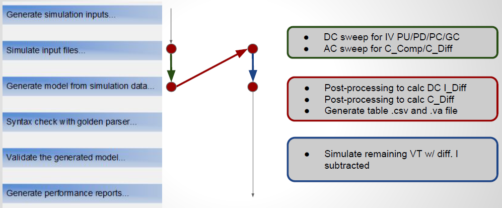
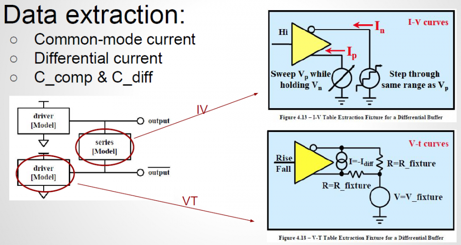
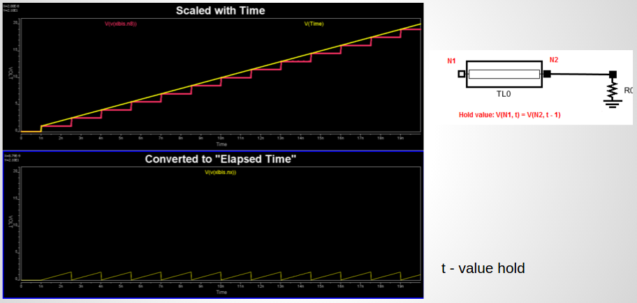
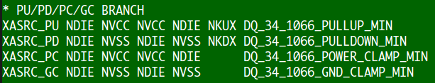
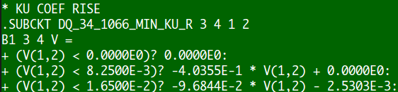
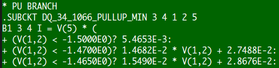
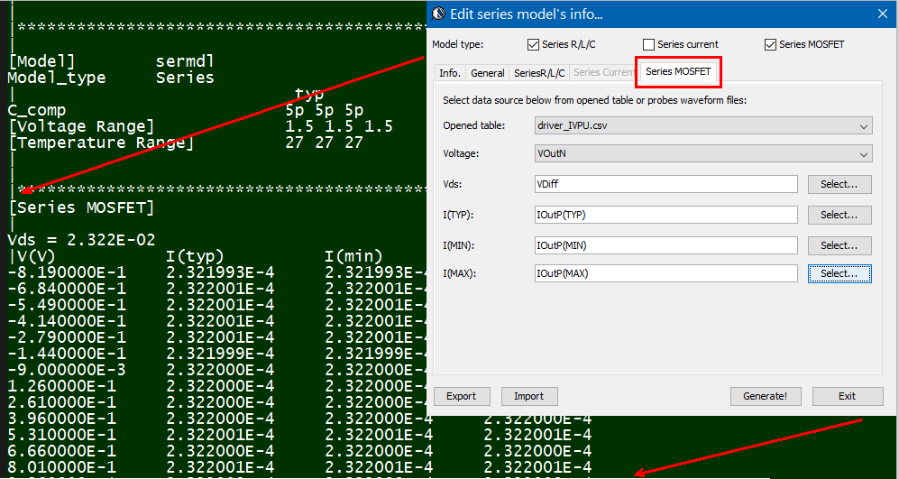
The same table content is sufficient to construct a series element. The steps needed here is to translate data into a IBIS compatible format. Such process is trivial when the model is simply R/L/C. For series current and series MOSFET (can have up to 100 tables of different bias condition), the attention needed to perform such work manually is not economical and a tool/flow should be used instead.

Modeling of the C-Diff:

CDiff

Similar process (tabulated and modeling) can be applied to calculated C_Diff. However, it’s much more limited in terms of series element’s syntax and E/F/G/H equation such that describing such surface (both frequency and voltage dependent) for C_Diff is not practical using either spice or series element. As a result, a trade-off needs to be made when picking values (or to average) from the surface and a single value is used when constructing model for C_Diff.

Verilog-A modeling:

In our submission to the IBIS summit later this year, we proposed another flow which is Verilog/VHDL based. One of the advantages of this implementation is that the raw, table-like data can be used directly using built-in $table_model function. Its usage also enables polarity differentiation and elaborated description of C_Diff, which is very crucial to the transient data accuracy. The details about this will be published here once our paper is accepted.

Combined model:

In previous post, we mentioned that in addition to the “series element” for differential model, pure [External Model] of the differential model type may also be used. Using the proposed Verilog-A/VHDL for series element only model, these two methods can then work together, as shown below:

CombSer

A series model is still declared in the “[Series PIn Mapping]” section to be connected between buffer’s N and P outputs. Its definition, can optionally include an external model such as the one implemented with behavioral language. This “[external model]”  works on top of existing series model definitions and can provide extra info. such as frequency/voltage dependent C_Diff if the simulator supports. Optionally, the “top” series model can be simply a  shell (e.g. with high impedance) and all the info. regarding the differential current is encapsulated inside the added model. When comparing to external model attached under output/IO buffer, this external model can be significantly less complicated and also provide more tuning capabilities.

Differential flow validation:

To validate a differential modeling flow,  one may construct a differential buffer by creating an artificial coupling (e.g. using some R/C elements) and then connect it between two known IBIS buffers. During the validation, the calculated common-mode data from DC sweep should reconstruct exactly the same PU/PD/PC/GC tables as those in the known IBIS buffer. Differential current will reveal the resitive element of the coupling portion. Calculated C_Diff should reveal the coupling capacitive element. Both of these steady state differential current and C_Diff can be validated using generated csv table or raw data. User should then find that with both captured accurately, the transient VT data calculated will also correlate to those of original IBIS buffer very well.

Paper and audio recording:

We presented this study at the 2016 Asian IBIS Summits. Readers may download the presentation from IBIS website or [HERE]. Audio recording at Tokyo is also available [HERE]

Differential modeling flow: Revisit

In the past, we have blogged several articles regarding buffer modeling. The flow and focus there are mainly for single-ended. The considerations are that:

  • Single ended (SE) buffer modeling is a good introduction to modeling flow in general without further complication;
  • (Pseudo) differential buffer can actually be modeled as two single-ended buffers;
  • Many (true/half) differential buffer can be modeled like pseudo differential buffer without significant loss of accuracy [LINK]
  • Differential buffer modeling involve several steps which are a little more complicated.

During our workshops in Taiwan last month, several attendees asked about CML (current-mode logic) modeling. With the maturing of the concepts in SE modeling and the prevalence of SERDES interfaces such as USB, SATA, PCIe etc, we think it’s a good time to revisit the differential modeling flow in more details. We will also show how this design concepts are realized in our SPIBPro in next post.

Note that the contents of this and next posts are also written in conjunction with the paper submission to the IBIS summit later this year.

Model descriptions:

[The info. here are summarized from the IBIS cookbook V4]

A differential buffer can be categorized into three different types:

  • Pseudo differential: shown in the rightmost of the picture below. The “P” and “N” driving portion are mutually independent. There is no coupling between these two pins in the circuit.
  • Half differential: shown in the middle. the pull-down portion of the “P” and “N” are coupled via a current source or shared load.
  • True differential: shown in the leftmost. Both the pull-up and pull-down circuits are coupled via “current-mirror” and shared current source.

DiffBuffer

For pseudo differential type buffer, the single ended buffer modeling flow can be applied directly. One only needs to generate these two “uncoupled” buffer separately (or use the same model with input flipped) and describe their differential behavior using the “diff pin” IBIS keyword:

DiffPin

Note that this “Diff Pin” keyword is also optional. So one may also simply instantiates two instance of the single ended buffer and use them together outside the IBIS file, such as in the spice netlist.

True/half differential buffer:

For a true/half differential buffers, the existence of “coupling” between P and N circuits must be described using existing IBIS syntax. There are two ways to do so: either using “series” or “external model” keywords:

  • Series: There are two places series needs to be declared: the first one is “[series pin mapping]” in the model headers and the other one is “series model” of the “coupling” circuit in the “[model]” descriptions:SerPin
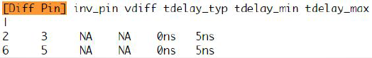
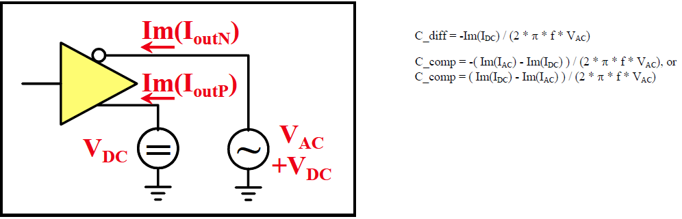
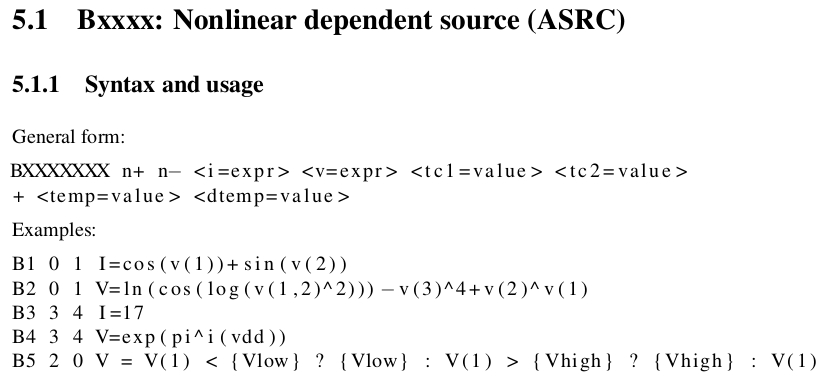
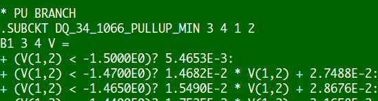
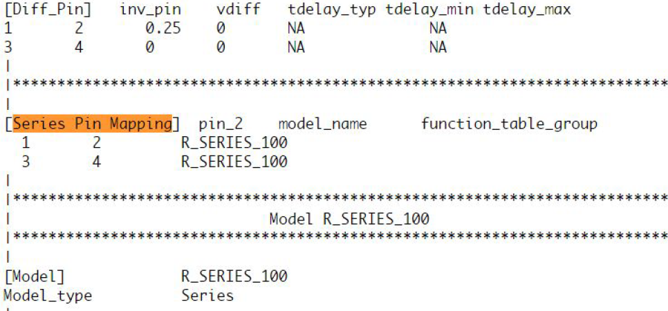
Take the picture shown above as an example. Under the “Series Pin Mapping” keyword, a model named “R_SERIES_100” is declared to connect pin 1 to and 2. Another instance of such model also sit between pin 3 and 4. Pin 1~4 each has its own model defined in other part of the ibis file already. For example, pin 1, 2 may have an output buffer connected while pin 3, 4 have open-drain buffers. This R_SERIES_100 model must have type “Series” defined as part of the IBIS file. Since “Series” is one of predefined IBIS model type, its contents (keywords) are not free form and must be one or more of the following series elements: R, L, C, Series current and Series MOSFET which contains up to 100 I/V tables under different biasing voltages.SerElem
  • External Model:  In the IBIS spec, four different differential specific model types are also support.:DiffMdlType
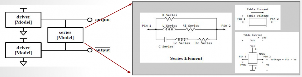
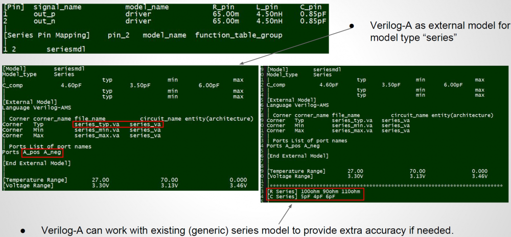
These differential model types must be implemented with language such as Spice, VHDL-AMS, Verlog-AMS, IBIS Interconnect Spice Sub-circuits (IBIS ISS) and declared with the “External” model section. These languages provides much more flexibility in terms of modeling capabilities, yet they also diminish the portability of the generated IBIS model.DiffMdlDesc
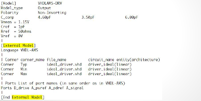
In the example above, a separate file “ideal_driver.vhd” must be provided outside the IBIS file and an “entity” of name “driver_ideal” needs to be defined. The port connections is described using reserved keywords after the “Ports” statement. In the IBIS Spec, all possible ports are pre-defined and the declaring order here must match their definitions in the associated Verilog/VHDL etc file.

Modeling process:

Pure method 2 implementation, i.e. coding in language like Verilog/VHDL, is up to the model developer. On the other hand, the syntax and structure of series elements, used in method 1, is strictly limited. Thus the modeling process below focuses on method 1 above, i.e. the series model method.

As the coupled half/true buffer described by separated single drivers and connected via a series model for the coupling, the modeling flow must somehow be able to extract the data for these blocks independently so that they can be described with conformed IBIS keyword and reproduce the response when putting together.

For the “Driver” block, it’s a generic input/output/IO type buffer. So tables such as pull-up/pull-down/power-clamp/ground-clamp, when applicable, must be extracted. So are the transient waveform under different test loads. The extraction must be done such that the coupling with other half can be separately as an independent “series element” model.DiffDrvDataExt

  • PU/PD: A two dimensional table produced by sweeping at both the P and N outputs are performed, as shown in the upper right block above. One major assumption for PU/PD extraction is that when both output pins are at the same voltage level, there will be no current flowing through the series model (i.e. the coupling portion). So in that condition, we can assume the series model does not exist at all. The current flows into or out of the buffer at that point is considered as “common-mode” current. This common-mode info is than extracted from surface table and modeled as pull-up and pull-down IV. The whole surface is then shifted vertically by subtracting this common-mode current at every x/y grids. The resulting surface table is considered as the differential current (resistance portion of the series model) and will affect the output when voltage at N and P are different. Note that to satisfy the aforementioned assumption of zero current through series element at common mode voltages, the sweep done at the P/N pins must step very slowly such that the charging/discharging of the reactive components, such as C_Comp or C_Diff can be neglected.
  • PC/GC: Clamp table in IBIS are always optional. On the other hand, when a circuit have current which always exist and can’t be turned-off, these data must go to PC/GC to avoid being double counted. That is, the PC/GC table must account for current which always exist and this current will be subtracted from the PU/PD table during the modeling process to avoid being double counted. Situations like this include the ESD circuitry and/or pull-up portion of the half-differential buffer. For PC/GC extraction, common mode sweep like that for PU/PD needs to be performed while buffer is disabled (put into high-Z state). The common mode current will then be extracted as the PC/GC table. Differential mode current is disregarded as it has been accounted for in the PU/PD differential data.DiffDrvCDifExt
  • C_Comp/C_Diff: An important step here is to extract and compute the differential capacitance, C_Diff. This has to be done before VT simulation. It is because C_Diff will affect the transient state differential current, thus it must be accounted for before VT transient simulation. The extracted value will be part of the series element model by adding as C_series. In real design, the C_Comp and C_Diff are both frequency and voltage dependent. So an user can perform 2D sweep in these two dimensions and select a proper value for C_Diff. This formula to calculate c_diff/c_comp is shown above.
  • VT waveform: With both static (resistive) data being processed from PU/PD/PC/GC simulation, and the reactive data, i.e. C_Diff, computed from the C_Die simulation. these two info can then be modeled together to be eliminated during VT simulation. The considerations is that: once the effect of coupling part is removed, then the remaining data can be considered as single ended and model accordingly. Having that said, reader should realize that there are much more details involved in this step. For example, how do you model these data? Two approaches may be considered:
    • Use E/F/G/H control element: the surface data can be fit to minimize the mean squared error. Resulting coefficients are then realized using poly function or like of a control sources.
    • Create a series element: decide the proper components and then create a series element.

Interested user may find some study presented in IBIS summit, such as [this one]

As one can see, the modeling process for a differential buffer is not linear and a certain order must be followed. Inaccurate common-mode extraction will affect IV tables and cause dc-mismatch of the steady state. In addition, failure to extract C_Diff and model different current accurately will greatly impact the accuracy of the transient data. We will see how a modeling flow should take these into account and be validated easily. These are also design concepts behind our SPIBPro flow.


Simulator development: Modeling (S & P)

System channel is usually represented in S-parameters. They can be extracted in frequency domain using a 3D field solver, and/or cascaded stage by stage using tool like SPISim’s SPro. With LTI (linear time invariant) assumption, it’s possible to synthesize eye or BER plot of millions of bits using statistically analysis… using single time domain pulse for these parameters. However, it’s still often desired to be able to simulate the s-parameter in time domain for defined bit patterns. Thus, a system simulator like our SSolve must be able to support such requirement. In addition, one may also want to know the frequency response when given a broadband spice converted spice elements, such as via, package or connector models. So the reversed process, i.e. extract S-parameters from spice elements, is also often required. In this post, we will briefly talk about how these may be developed in simulator like SSolver.

S-Element… S-Parameters:

There have been many conference and journal papers proposing different methods of simulating S-parameter in time domain. However, at the most basic level, S-parameter can be considered as a transfer function or filter block. Thus DSP techniques can apply: transfer function multiplying inputs in frequency domain can be converted into time domain using convolution:

Convolusion

The time domain at the right hand side can be further separated into two parts: history up to this time point (integrate from -infinity to t=n-1) and the value at this particular moment t=n due to input. The first part is a constant as it’s already happened in the past and can’t be changed, the second part is, however, input dependent and must be updated within the “solve” and “stamp” hot loop inside newton iteration. When putting together, they form a Norton circuit form of I = Y * V + J where Y is value affected at this moment and J, a constant, is due to past history. This Norton form can then be “stamped” accordingly for matrix solving.

Interested reader may refer to the paper published by HP linked below for detailed explanations and math:

Integration of Transient S-Parameter Simulation into HSpice

The equation [18] and [19] is the aforementioned Norton equivalent circuit form and can be used accordingly.

The convolution method needs to update history with the solved results of this time step for next time step to be used. In addition, the basic convolution requires that the dt to be constant, thus a variable time step simulation will be greatly hampered by this requirement in terms of performance. So the convolution modeling has rooms for improvement.

One of the possible approach is using vector fitting technique mentioned in previous post about “W-element” modeling. With the S-parameter data in frequency domain, one may construct a Pade approximation using several poles and zeros. Then basis functions can be created for each of the pole in time domain and simulate accordingly. A benefit of this process is that the constructed form is a rational function which is guaranteed to be causal. So if there are issue regarding causality of the provided s-parameter, it can be fixed during the modeling process. Lastly, due to exact fitting of multi-port s-parameter across the frequency spectrum are not likely, some sort of error minimization (in the MSE sense) is needed to have a balance between accuracy and number of poles.


P-Element… Port element:

Often times after a package, connector or via modeling engineer created a model, he or she will use tool like broadband spice to convert such 3D extracted s-parameters to spice equivalent circuit composed of various basic elements. When a system designer or SI engineer receive such converted models, the original S-parameter may not be available already. Rather than insert this model into the channel and simulate blindly, it’s often beneficial to be able to reconstruct and inspect the model’s frequency domain response first before actually using them. S-Parameter extraction via simulation is basically a form of AC simulation, thus with AC model of the system elements constructed, the S-Parameter extraction part becomes easy.

The context here is small signal S-parameter extraction, thus all the AC signal is done very close to the operating point. That is, a DC solution needs to be obtained first for each port’s respecitve bias condition, then the AC stimulus is applied and solve for each frequency point.

A “Port” or “P-element” has several properties: dc bias condition, reference impedance, port-name and port-order. For a multi-port s-parameter extraction, one port is excited at a time with specified dc bias value. AC sweep is then performed while the other ports are terminated to their reference impedance. The power wave of input and output, measured and processed using current injection and nodal voltage measured, can then obtained for this input to the other output ports. Using simple math described in the link below:

S-parameter measurements

one can obtain S-parameter of Sij (i is port with input stimulus, j are the other ports) content easily this way. Repeat the same process for the other ports one at a time (with their respective dc bias condition) and the full S-parameter can be obtained. Finally, the order of ports are arranged according to the port properties, their respective port name are written out at the top of the touch stone file and the process is complete. Should there be needs to convert to other formats such as Y, Z parameter (sometimes good for checking connectivity), one can do so easily with formula (assuming generalized 2-N ports) or simply use developed tool like our SPro.


Back to the top:

Back from these modeling physics to the computer science domain, one also need to consider the following topics when doing simulator development:

  • Memory pool management (allocation, expansion and clean-up)
  • Multi-threading consideration
  • Plug-in architecture for future devices
  • ….

While the list can go on and on and the tasks may be daunting, the end results are definitely worthy to the analysis flow and methodologies development. With developed simulator, there is no longer absolute need to form a close-loop formula or equation in order to solve circuit equation. The module or flow running on top can simply create netlist and have this simulator solved for you. Not to mentioned this also make maintenance and testing much easier. For an EDA company like us, I would say this is a journey worth taking.

Simulator development: Modeling (B & W)

When modeling device for a circuit simulator, the raw netlist input needs to be converted into internal structure first, then a physical model is constructed during the “modeling” phase, and corresponding equivalent Norton or Thevenin circuits’ parameter are solved within each Newton iteration at each timestep. The solved parameters are finally “stamped”  into system matrix for Newton iteration solving. “Model” and “Solve” is the essential part of device modeling for a circuit simulator and that’s whey “Physics” come into play.

In these two posts, we will briefly talk about how system devices, in particular IBIS, Transmission line and S-parameter are “modeled” and “solved”.

B-Element… IBIS:

Looking at the IBIS’s structure, the modeling part is actually quite straight forward:

IBISEvolve

The four IV curve data: pull-up, pull-down, power clamp and ground clamp act like non-linear resistors. With terminal voltage known within each Newton iteration, the conductance can be look-up from these curve tables and obtained using linear interpolation.

The switching coefficients and composite currents are both time dependent. Their values are calculated in the “modeling” phase when simulation has not even started. The obtained coefficients is a multiplier which will further scale the conductance calculated for IV data and thus stamped value. These scaling are such that when test load specified in the waveform section is connected, driver at the pin will reproduce exactly the same waveform data given in the model. As to C-Comp, it can be inserted using simulator’s existing infrastructure so the integrator there will manage the stamping and error prediction.

The more complicated portion of IBIS modeling inside a simulator is due to the options available for the end user, thus model developer must plan in advance. For example, the c_comp may be split across different terminals. Each waveform, IV or components have different skews which book-keeping codes must take care of. There might be added submodel for pre-emphasis or de-emphasis so the class implementation-wise one should consider “composite” pattern such that recursive inclusion can happen. At the end, this is a relative simple device to model for simulator, particular when comparing to the transmission line.


W-Element… Transmission line:

Every electromagnetic text book will give transmission line structure as shown below:

RLGC

This is an uniform distributed model and is implemented early in various simulators as  the “U” element. While implements T-Line model this way is now outdated due to the performance issue, it’s still how the T-Line’s raw data, frequency dependent tabular model, are given:

TabModel

The tabular model are field solved of Maxwell’s equations based on layer stackup, trace layout, material properties and sometime special treatment (like surface roughness) and finally presented as R/L/G/C data at low (DC), high (Infinity) frequencies and many points in between. Thus to model T-Line for a simulator to use, one has to convert these data to a mathematical form first which can then be used in either time or frequency domain. For transmission line, this can starts with Telegrapher’s equations.

By solving the KCL/KVL of a unit length RLGC circuit above, one can derive and find the telegrapher’s equation:

And the solution to this equations, as explained in the wiki link above, involve a wave propagation function Gamma:

RLGCEq2

When realize this in the system model, it as the Norton equivalent circuit form:

So on each side (near end and far end) of the transmission line, there are two components: Z (admittance) at that particular time step and current source due to the propagation delay originated from the other end. These two components (Z(s) and r(s)) can be obtained from the tabular data in frequency domain and then converted to integrate-able form in time domain so that they can be “stamped”. Generally, it includes the following steps:

  • Parse and store the raw tabular model;
  • Calculate the propagation delay and characteristic impedance using highest frequency data (or using extrapolation), these value will be used for interpolation later in time domain.
  • Construct the Z(s) or Y(s) and the wave function r(s) shown in the system model. As transmission lines are usually coupled, these curves are multi-dimensional in frequency domain;
  • Using vector fitting technique to represent this frequency domain functions using series of poles and zeros. In most of the cases, particular when the model data has insufficient bandwidth or low quality, exact fit is not possible with reasonable number of poles/zeros and thus best fit in the minimum-square-error sense needs to be performed.
  • Once pole and zeros are found, they can be converted into time domain as different order of terms. All these terms combined together will form the Y(t) or r(t) in time domain. Pade’s approximation may be used here.
  • During time domain simulation, use interpolation to find r(t)’s value in the past history (propagation delay ago) and use that data to construct the equivalent model of this end at this particular time point.
  • For frequency domain analysis, vector fitting and conversion to integral form is not needed. The Y(s) and r(s) data can be used directly for stamping at this frequency with some interpolation.

For the first three steps, I wrote a simple matlab codes to demonstrate how how they are done:

Impedance function:MatlabY

Propagation function:MatlabH

Plots:PlotY

PlotH

While the matlab codes above seems straightforward,  most simulator (including SPISim’s SSolver) will program with native codes (C/C++) for performance consideration. So a whole lots of matrix operation (inverse, eigen value, LU decomposition etc) will also come into play during the process.

It’s rarely the case that the developed model or codes will work the first try. With so many terms (of converted poles and zeros) for so many dimensions (coupled cases), it’s a daunting task to figure out what has gone wrong when waveform is not as expected. It’s often simpler to back to basic: check steady state solution first, use one line, no reflection with by matching impedance at the other end, use characteristic impedance to find nominal reflection value and so on to help identifying the issue:

TLDebug

Interested reader may find more details about SPISim’s implementation, same as HSpice’s, in the following paper:

“Optimal Transient Simulation of Transmission Lines” by Dmitri Borisovich Kuznetsov, Jose E. Schutt-Aine, IEEE Trans. on Circuit and Systems, I Feb. 1996

In terms of book, I have found that Chap. 5 of Dan Oh’s “High-speed Signaling” book, S6 in our reference book section, give best explanations among others. This maybe because Mr. Oh is from UIUC around the same time when the paper was published as well 🙂 It also worth mentioning that similar technique can be applied to other passive, homogeneous device modeling, such as the system channel. For example,  one common approach of checking and fixing casual issue of a s-parameter is by using vector fitting and convert to rational function form.

Simulate IBIS Data with Free Spice [Q & A]

I presented our developed “Ibis to Spice” flow last week at the IBIS summit of 2016 DesignCon. It was well received. In this post, I recapture discussions raised in the Q & A section for those who didn’t attend the summit.

  • Q: Does free spice have IBIS parser?
    • A: Nope. Neither NgSpice nor other free spice simulators that I am aware of come with IBIS parser. As a matter of fact, none of the free spice supports IBIS model at this moment. However, interested user may see what pyIBIS has offered and make use accordingly. Lastly, accordingly to the IBIS website, one can pay about $2500 and obtain source codes of golden parser. In our tool, we do have built-in IBIS parser implemented in cross-platform format to support this Ibis to spice conversion flow.
  • Q: Where is ASRC? I can’t find it in Berkeley Spice 3f5’s manual.
    • A: Please try NgSpice instead. Free spice simulator like NgSpice, EiSpice, LTSpice or even TISpice are all Berkeley spice derivatives. Their syntax may be deviates a little bit but the proposed algorithm should work on these simulators with very small syntax changes.
  • Q: Does this template only work for buffer with symmetric rising and falling?
    • A: Not true. The template we have developed will digitize the analog input to a digital one… one with very sharp rising/falling edges. The detection is based on a voltage threshold. So it does not matter whether the rising and falling time of inputs are symmetric or not.
  • Q: Can this spice template account for buffer overclocking?
    • A: IBIS spec does not specify how a circuit simulator should behave when a buffer is overclocked. So the results of a overclocked buffer maybe already circuit simulator dependent. Ideally, a mechanism will make sure current contributed by the pull-up/pull-down branches stays continuous during buffer clocking. This way voltage will also be continuous instead of sudden jump or drop. I suppose a more complicated mechanism can be added to the template to account for situations like these. However, it is not there at this moment.
  • Q: Will there be any issue if I simulate the buffer very long, say for 1us?
    • A: If the parameter used in ASRC element is too small, for example the original value of time “t” used by switching coefficients, then it will be rounded and cause incorrect results. This is because we usually use ps range as time step. That’s why we scale the value up in the template and also account for for this scaling in the pre-calculated Ku/Kd coefficients. If the scaling is 1E9 (as based line for for 1ns), then 1ps will becomes 1E-3 and 1us will be 1E3, both should not be rounded by the simulator. Thus I think this approach should work for long simulation time, such as 1us.
  • Q: Why is T-Line needed? Isn’t it the case that simulator has buffer history which can be accessed for the same reason?
    • A: Yes, most of circuit simulators have a buffer to record nodal voltage history. This way if one decides to use Trapezoidal rule to calculate first derivative, the previous two points can be used. Note that I am using purely spice syntax and element to mimic the dv/dt and delay effect. I have no access to the underlying C/C++ buffer structure, that’s why lossless T-Line is used. With this approach, if one want to get history data of more than one time step before, cascaded T-Line can be used. At each junction of the T-Elements stores the voltage history of previous n time steps (each T-element is one time step delay long).
  • Q: Why is “fine tuning” for handing off needed? Ku/Kd should have reached steady state already before transition.
    • A: When buffer is not overclocked, Ku/Kd will reach its steady states. For example, Kur will be come 1.0 at the end of rising transition so that pull-up branch is fully “ON”, while Kdr will becomes 0.0 so that pull-down branch is fully “off”. The reason we need the “fine tuning” to make sure “handing-off” between Kur and Kuf (Kdr, Kdf) is smooth is purely due to the spice syntax based implementation. Theoretically, it’s not needed. User may take the provided template and comment out the “fine-tuning” section and observe the spikes. If you find out other simpler method to filter out these spikes, please let me know.
  • Q: What is next step?
    • A: We plan to continue the path to support system simulation using free spice. Take NgSpice as an example, there are three approaches to add support for a new device, such as IBIS:
      1. Add as a native device like R, L, C: this requires knowledge of circuit simulator algorithm, the code structure and flow. Developer needs to codes in c and extend the arrays of existing device structure. It requires lots of effort and may take longer time to complete.
      2. Add a code-model library using XSpice extension: this requires knowledge of XSpice extension to NgSpice. Developer still needs to code in c still and compile code model as dynamic linked library, but the structure and flow is limited to XSpice device. There is no need to touch underlying spice infrastructure. It’s easier comparing to approach “1”. The compiled library is platform and os dependent, and is a little bit tedious in debugging (need to attach to a running process as the code model is loaded library). However, the developed code model library can run on any existing or released NgSpice simulator.
      3. Use ASRC element to model the behavior outside the simulator: This is what we have accomplished so far. It works well but performance is not that great.

In current version of NgSpice, IBIS, W-element and S-parameter device needs to be added to support system analysis. We plan to continue to approach “2” above and provide support of these devices in the form of  code-model library.

Simulate IBIS Data with Free Spice [Part 2]

Note:

Interested reader of this post may also want to follow up with the [Part 1] of same topic and try out the [Free Web App] which realizes this conversion flow.

For the motivation behind our Ibis to spice development and Ramp based Ibis2Spice conversion flow, please see [previous post]

Waveform based Ibis2Spice conversion:

Typical IBIS model simulation makes use of its waveform data. Thus a converted spice model from its IBIS model must be able to use these timing related data to have good correlations .

Both voltage and current related data can be timing related: In IBIS model of version 3.2 and up, one ore more “rising” and “falling” waveform may be included. Typically, two set of waveform under two different loading condition will be provided. In case only one waveform is available, simulator may convert ramp data to form additional set of waveform. In IBIS model version 5.1 and up, “composite current” is also included in order to account for simultaneous switching noise. This current information is point-to-point aligned with their voltage counterpart to withdraw current from power supply terminals of the buffer model. Note that what we call “timing” here is actually “elapsed time” after buffer’s input signal switches from low to high or high to low. Two sets of switching coefficients, Ku/Kd for rise and fall transition respectively, are used to mimic the gradually turning on/off the PU/PD branches such that under test load condition, the voltage and current waveform data can be reproduced accurately. By using these swtching coefficients, buffer’s strength will be scaled accordingly depending on the load. User may see [our past s post] for buffer’s operation in more details.

Once we have the related  info. then we can create building blocks and assembled exactly as  they are meant to be used in IBIS model, but now in spice format. So the schematic of our waveform based converted spice model will look exactly like a “stock” IBIS:

Selection_209

To achieve this, i.e. be able to use timing data in converted spice model and run like a stock IBIS, three main challenges need to be overcome:

  • Extract “elapsed time” info. during simulation;
  • Compute the switching coefficients Ku(t)/Kd(t) for both rise and fall transitions;
  • Assembled the block together and mimic actual IBIS operation.

Extract “elapsed time” info. during simulation:

In free spice (e.g. NgSpice)’s ASRC (Arbitrary SouRCe) element, function can be used.  One function parameter which may be used for this timing purpose is the “time” variable:

Selection_210

By using this “time” variable, we can calculate and extract the “elapsed time” info.:

  1. First, we need to be able to differentiate between rising and falling from input. This is because both rising and falling transition needs its own Ku(t)/Kd(t) table. After converting input analog to a digital signal, we can use first directive such that rising and falling can be differentiated. To compute dv/dt, a transmission line (TLine) can be used. Other choice may include using a Laplace equation in control element to mimic the “delay”. The decision of using TLine for the delay is also because in free spice, the control element does not support “delay” parameter like other commercial simulator does. Measurement of voltage differentials across TLine gives us dv and TLine delay is a single simulation step dT. TLine is terminated with its characteristic impedance so no reflection will incur at the far end.Selection_211
  2.  Once rising and falling transitions are separated, we can multiply the converted dv/dt with “time” variable and also use a “latch” to hold the signal at the end of the transition. Again, we use a matched TLine as a “latch”: by feeding near end voltage with the far end one, which is data of previous time step, we can have a latch holding signal indefinitely. The latched signal is show in red of the upper plot below. With another “time” variable subtracting this latched signal, we can then obtain “elapsed” time as show in the lower half of the plot. One caveat is that in typical time domain simulation for SI/PI, time step is pico-second range. Spice will ignore variables of very small value, such as 1E-12 scale, thus a proper scaling will be necessary.Selection_212

Compute the switching coefficients Ku(t)/Kd(t):

With the elapsed time, t, now available, we can compute Ku(t)/Kd(t). There are numerous paper and presentation detailing the algorithms. For example, one may compute this switching coefficients from model data based on the first reference below, or use measured based approach based on spice simulation detailed in second reference:

  1. Extraction of Transient Behavioral Model of Digital I/O Buffers from IBIS, Peivand Tehrani et. al, 1996 Electronic Components and Technology Conference.
  2. General K-table Extraction w/ Spice, Bob Ross, IBIS Summit, DesignCon 2015

In general, waveform data from two different test loads are used to solve two unknowns at each time points during rising/falling transition. This calculation is done offline in advance and the resulting data are again realized in the form of ASRC devices. The PU/PD/PC/GC branches will be exactly PWL based ASRC, only that the PU/PD takes one more input (NKUX, NKDX below) which is the switching coefficients, Ku(t) and Kd(t):Selection_205

Ku/Kd are ASRC with pre-computed coefficients and variable of “elapsed time” computed from the first step:Selection_206

PU/PD branches draw associated  current based on the Ku/Kd value presented as voltage value at node 5 below:Selection_207

Assembled the block together in spice formats:

While netlisting different PU/PD/PC/GC/Ku/Kd blocks together is trivial, a nuance becomes apparent during validation: the assembled spice model will have “spikes” right before and after each transitions which makes the model unusable.

Further investigation reveals how devil is hiding in such details… As explained in our previous post, there is a “hand-off” during transitions:

That is, when we “run out of” Ku/Kd for, say rising transition, we keep using the last point data until buffer is about to switch from high to low state. At that point, “hand-off” happens so that Ku/Kd for falling transition will be used. The “hand-off” process is triggered from input and even a time step delay in terms of table usage switching will cause huge spike and cause problem. With carefully looking into different signals in details and figure out their relation in timing, we have a solution which filters out all the spikes and produce a well correlated results, as shown below:

Selection_202

Both the voltage waveform and drawing current matches quite well. The small delay is insignificant because it’s a constant added to each cycle and will be eliminated in the eye plot.

As we introduce two single time step delay transmission line elements to calculate dv/dt and serve as sample-and-hold functions, they also limit the simulation time step a simulator can take. As a result, the converted model run much slower compare to its IBIS counterpart run in other commercial simulator under test load condition. In extracted channel simulation, the “slow down” becomes less apparent as there are multiple transmission line segments present in the topology. The time step limit introduced by the shortest transmission line is common to all simulators which may not be much longer than the TLines we have introduced.

Another note worth mentioning is that while this post focuses mainly about Ku/Kd and voltage waveform data, Composite current and their ISSO_PU/ISSO_PD are treated similarly: An ASRC constructed from composite current based on time aligned point with voltage counterpart is used to draw current. Another set of scaling table, based on ISSO data ares computed off line in advance in order to take the non-ideal voltage supply into account.

With both ramp and waveform based Ibis to spice flow being available, we are able to perform SI/PI simulation using IBIS on free spice simulators. Such flow has been integrated in our SPIBPro flow as shown below:

Ibis to Spice function is SPIBPro

Ibis to Spice function is SPIBPro

This post is written in preparation for the upcoming IBIS Summit at DesignCon 2016, where we will present this Ibis to spice flow. The presented slides and associated examples are shown below. Reader may also download them from IBIS's official page for this summit.

Presented slides: View externally [HERE]

Example files: [click to download]

Simulate IBIS Data with Free Spice [Part 1]

Note:

Interested reader of this post may also want to follow up with the [Part 2] of same topic and try out the [Free Web App] which realizes this conversion flow.

IBIS to Spice:

Most of the buffer modeling flows focus on creating IBIS models from existing transistor buffer design, usually in spice format. However, we also find values in  flow of doing the other way around, namely converting IBIS model to spice format. This is motivated by one or more of the following reasons:

  • System SI/PI analysis support with free spice simulators: There are several simulators, e.g. Berkeley 3f5, eispice, ngspice, LTspice, available in public domain or free of charge. Due to historical reasons, their focus tends to be more on-chip or vendor products specific, like BSim3/4 for Berkeley spice and voltage regulator for LTspice. While they all have certain degree of transmission line support, yet when it comes to IBIS portion, they are totally lack of. Without driver model, which usually comes in the form of IBIS models, one can’t perform system analysis! It’s certainly possible to develop native IBIS support into these simulators, but the immediate available solution is to have a flow to convert existing IBIS model into sub-circuit like format and be able to simulated in these simulators. The added benefit of this approach is that engineer who has ad-hoc need to run SI/PI simulations with IBIS involved can do so quickly with these free available simulators without incurring much overheads.
  • Vendor neutral release of IBIS reference data: IBIS is a non-proprietary data format. When implemented correctly, simulation results from different simulator vendors should correlate with each other very well. To help achieving this, “golden waveform” data can be part of the IBIS model release. In reality, the “golden waveform” is optional and each simulator vendor’s implementation is different, thus the results may be different. We have seem model providers, such as Micron etc, also provide encrypted hspice as part of  the release to provide “golden reference” for the IBIS model. The disadvantage is that encrypted model needs to be run on proprietary simulator which is usually not free. So there is a value to be able to release IBIS, its corresponding data in non encrypted form AND allow user to validate the model with public domain simulator as well. This also encourages (simulator) vendor neutral model release.
  • Explicit IBIS algorithms implementation for educational purpose: There have been many papers and presentations detailing usage of IBIS data inside a circuit simulator. While it’s good for high-level overview, the truth is that these algorithms are often implemented deep inside a circuit simulator. With the developed Ibis to spice flow, we expose these algorithm in the form of plain text (versus C/C++/other programming language) spice compatible subckt format. We believe it will  be very educational and have much reference value.
  • Speed up flow development: Circuit simulator is one of the back-bone of SI/PI analysis (field solver can be one of the others).  To be able to use simulator as part of the developed flow, several options are possible: 1. choose to work with established simulator vendor and require customers to have license accordingly, 2. develop one internally, or 3. make use of tried and proven ones in public domain. Each of these approaches has their pros and cons. As a start-up company focusing on providing flows of high C/P (Performance/Cost) value, we would like to save the cost of other licenses and development efforts for our customers and speed-up the development when possible, thus option 3 is a very attractive solution to us.

There is already a vendor providing Ibis2Spice in their tool. Their free version supports only up to V2.1 IBIS model and the paid version only up to V3.2 IBIS model. Having that said, the model converted by their tool can’t be simulated in free spice directly. The flow we have developed can supports up to V5.1 model which includes the current information like [ISSO] and [Composite Current] keywords. In these two posts, we will explain about our flow in details. We will first review how ramp rate data can be used in free spice, followed by how waveform data can be converted into spice, accompanied with correlation data in both cases.

Goal of developed flow:

  • Run on free simulator, e.g. Spice3F5 and NgSpice
  • Support VT waveform data (IBIS V3.2 and up) and current data as well (IBIS V5.1 and up)
  • Produce very good correlation compare to commercial IBIS implementation.

Ramp based Ibis2Spice conversion:

In this first post, we will review the existing Ibis2Spice flow. We have also re-implemented this IBIS to Spice flow and release it free in our SPILite module. Output from our flow is directly usable in free NgSpice, which is also included in our tool. Basically, it uses ramp rate data only in the given IBIS model and creates a corresponding spice model. The learning here is how behavior source, ASRC (Arbitrary SouRCe) can be used to implement the IV table lookup. This technique will be applied more extensively in waveform based Ibis to spice flow (next post).

Searching from the web will bring you to this post (for original author’s credit): IBIS to Spice Translation (part 1). In this post, author describes the operation, his attempt to modified circuit and the result. He also provided an Awk script to accommodate the the changes needs to be made in order to run on free spice. As this post is written more than twelve years ago, part of the content has been outdated. For example, the NgSpice 26 does accept the syntax like  X + -3.12 so there is no need to convert to X-3.12 any more.

The part 2 of the original post show the schematic of the converted ramp-based spice circuit. It is hard to find on the web, so we post it below to save reader’s effort:

Ibis2Spice Schematic

The key elements here are four IV curve data: XPWRCLAMP, XGNDCLAMP, XPULLUP and XPULLDOWN. These four IV tables from original IBIS have been realized with ASRC sources, as explained in NgSpice manual:

Selection_195

The power clamp and ground clamp branches are always on, so the data is used directly. Their ASRC data is a converted PWL curve shown below. Depending on terminal voltage V(1, 2), current will be output or drawn from terminal 3 and 4.

Selection_199

For pull up  (PU) and pull down branches (PD), they are turned on/off only after buffer has switched, the rate of turning on/off is based on a RC constant (C1 and RB3 in the upper left of the schematic) converted from ramp rate value in the model. This RC value is then used to multiply the PU/PD voltage and finally converted to a current source using G element (VCCS, Voltage Controlled Current Source).

Selection_197

Selection_198

In the original post, author mentioned he has attempted to replace this RC based implementation with his PWL version yet get non-smooth results. We think this is because PU/PD branches are turned-on/off gradually. Only when they are left for certain period of time, static state will be reached. Thus a “time” based parameter must be present. Otherwise, static solution is solved at each time step and thus result will be incorrect. RC multiplier realizes this transition of “gradually” turning on/off the PU/PD branches.

With the RC based implementation, one can mimic the “ramp” data used in other IBIS capable simulator and produce good correlation, as shown below. Due to the simplicity of this implementation, the simulation speed is very fast.

Selection_201

Note that with this implementation, drawing current from VCC/VSS are way off. This is also indicated in the original post. As a result, this approach will not be useful for SSN simulation which includes PDN noise. Further more, it will not capture initial undershoot, final overshoot and other more subtle waveform presented in real buffer switching, also the RC curve (shown in the red above) is not true “linear”. In additional to the ASRC based implementation for IV tables explained above, part of the converted circuit is used to detect and convert input analog signal into digital ones. Lastly, each corner of the model to be used in the simulation needs to have a spice subckt library converted from corresponding corner in original IBIS model.

This post is written in preparation for the upcoming IBIS Summit at DesignCon 2016, where we will present this Ibis to spice flow. Please see the [Part2] and download presented slides and associated example files.

Transmission Line Model: Layer stackup and T-Line fundamentals

Most parts of the channel between driver and receiver, usually in the form of multi-segment transmission lines connected together or through different vias, reside on different layers of PCB. Thus it’s important to understand how these layers and transmission lines are modeled for signal/power integrity analysis.

Layer stackup:

A print circuit board (PCB) is usually composed of multiple layers in a modern system. Several sheets of cooper wrapped cores are bonded together with pre-preg in between to form multiple layers. The core and pre-preg are dielectric materials and coppers serve as medium of conducting plane and traces. Copper’s height is often represented by weight in terms of oz, and dielectric is made off lame retardant material (FR4). Depending on the number of routing and plane layers needed, common PCBs are often 6, 8, and 10 layers for desktop or mobile application. Both material and geometry properties of stackup and traces are quite homogeneous and can be simulated with 2D field solver.

Different conducting layers are connected with “via”, which is a barrel of conducting plate and pads/anti-pads at different layers. There are several different types of vias: PTH for plate through hole from top to bottom layers, blind layers (originates from top or bottom and ends at inner layer) and buried via. Via structures are usually non-uniform and require 3D field solver to model, thus is not included in the discussion in the layer/transmission line context.

Layers of copper+core are bonded together...

Layers of copper+core are bonded together…

Different types of vias

Different types of vias


Transmission line (T-Line):

Some of the conducting layers in the multi-layer PCB are used for signal traces routing. Depending on which layer they are, different relations respect to the adjacent reference plane may be formed: Microstrip, Stripline and Dual stripline.

Types of traces

Types of traces

In terms of circuit modeling, each short segment of such traces can be represented as a RLGC lumped element. The values of R/L/G/C depends on the cooper conductivity, surrounding dielectric’s permittivity, loss tangent and trace’s geometric properties such as width, height and distance to the reference plan. When propagation time through such small segment is longer than one tenth of the signal rise time, then lumped model is no longer valid. One must use Maxwell equations to explain the signal propagation behavior along this signal trace. Having that said, the circuit model of non-lumped transmission line is still represented by R/L/G/C values or matrices solved by field solver with aforementioned material and geometrical properties according to the Maxwell equations.

LumpedEq

Lumped model and T-Line equation


T-Line performance parameters:

Several performance parameters can be defined based on a T-Line’s R/L/G/C model to describe its properties:

  • Impedance:  Energy may be partially reflected at the boundary where impedance becomes discontinuous or mismatched. This is one of dominate factors in signal integrity problems called inter-symbol interference (ISI). Thus a quick scan of characteristic impedance of signal traces along the path can reveal many useful information why signal deteriorates.
  • Crosstalk: While diagonal terms of R/L/G/C matrices explains the relationship of trace itself to the reference plan, the off-diagonal portion explains the interactions between different traces. The energy is shared between these traces because of the EM fields and thus a nearby aggressor can often cause victim’s signal integrity problem particular when they run in parallel for very long distance.
  • Propagation delay and attenuation: These are often secondary factors when comparing to impedance and crosstalk. Signal of different frequencies propagate at different speed and suffer from different degrees of attenuation, both contribute to the deterioration of signal.
Extract performance parameters from a T-Line's model

Extract performance parameters from a T-Line’s model


Stackup and T-Line modeling:

There are often trade-offs between layer stackup and routing T-Line when designing a system. For example, the PCB cost is reduced with fewer layer count yet dense routing or narrow trace width may incur more crosstalk or higher impedance. Also, how to plan trace geometries to make sure impedance is well matched along the channel? All these may need detailed planning in advance before traces or components are lay out. Thus the purpose of stackup and T-Line modeling is to explore the relationship of costs (in terms of layer count or dimensions etc) vs trace performances.

As both material and geometrical properties comes into play, on top of different trace type (microstip, strip-line etc), there are many factors to consider and one needs to identify primary ones vs performance. Basic steps may include:

  • Decide layer counts and where the traces will be routed
  • Decide material and geometry variables for the layers and traces
  • Generate a simulation plan to sweep across these parameters
  • Execute the sweep plan using field solver and obtain traces’ RLGC models
  • Extract performance parameters and map input variables to these targets
  • Identify whether this mapping (prediction model) contains desired solution
  • Go to step one and try different layer configuration if needed.
Layer and trace modeling

Layer and trace modeling

If the layer configuration is used often, one may also record the mapping model as prediction formula for future use. Our experience has shown that such models usually do not require higher order (>2) terms and are very well behaved for prediction purpose.

Prediction model

Prediction model