Given one or more IBIS models, if all of them passed golden parser and meet my speed requirements, how do we know which one will be best fit for my channel? In this post, we are going to propose several IBIS performance parameters. It’s out hope that with these parameters, we can easily make comparison between different IBIS models and will pick the best candidate for our high speed design need.
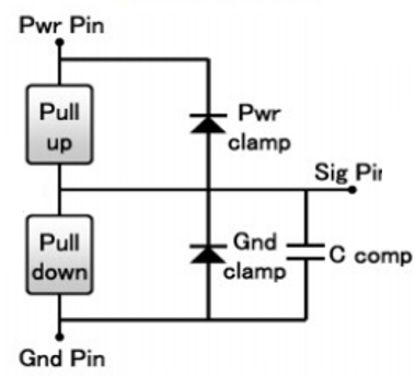
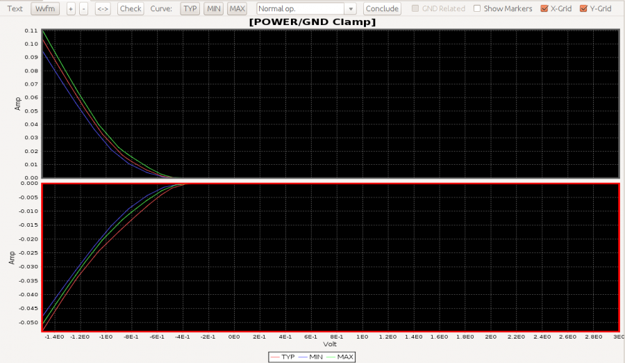
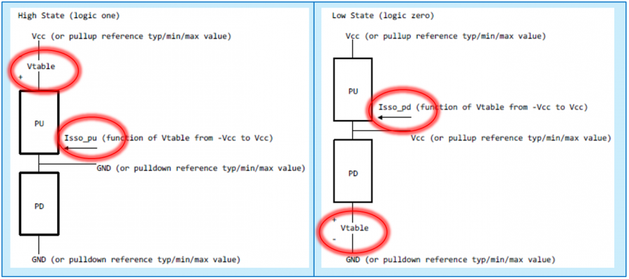
The basic IBIS data structure is shown above, which we should have been familiar with by now. There is both pull-up (PU) and pull-down (PD) circuits which will decide the steady state output impedance. There are ESD circuits represented by power clamp (PC) and ground clamp (GC) which operates in reverse bias condition normally. How fast the PU turns from OFF to ON state and PD from ON to OFF state determines how the transient rising response of this buffer is, similar for the falling state. Due to the reverse bias condition of PC/GC, the leakage current is usually very small.

Another situation is like the figure above. In this case, there are on-die termination associated with buffer. Thus the current when buffer is in high-Z state will be significant…much larger than the leakage current of PC and GC.
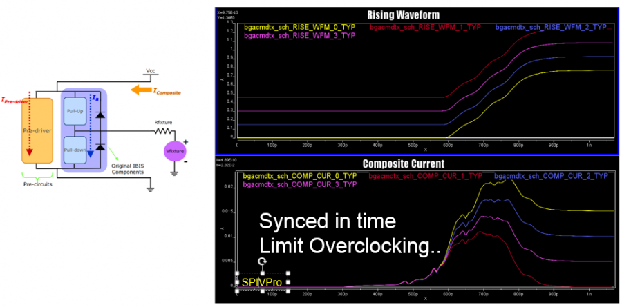
From these two common usage scenarios, it seems reasonable that we can use both output impedance and timing response, represented by rise/fall time and slew rate as bases for our IBIS model performance parameters.
IBIS output impedance:
If the buffer’s output impedance does not match immediate connected output, usually the break out region of package represented by transmission lines. There will be significant reflection and cause damage the signal quality from the very beginning. The usual remedy is to add a series resistor such that the total output impedance will match 50 ohms, the usual characteristics impedance of a transmission line. The figure below show a typical ringing caused by impedance mismatch.

Note that the PU and PD may have different impedance value around reference voltage, say 50% of Vcc, thus one common choice of series resistor to be added is the average of PU/PD impedance around that region.
IBIS timing parameters:
For better signal integrity, it is usually desired to have just fast enough signal with smooth transition edge, rather than fast signal like square wave. We have all seen the following decomposition of a square wave, as shown below. Starting with pure sin wave with same fundamental frequency, the more harmonics are added together, the more the resulting waveform will look like a square wave.
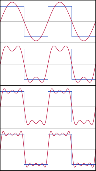
Signals of different frequencies will have different traveling speed along the propagation medium, thus cause the signal distortion. This phenomena has a special term called “dispersion”. So the slower the rising edge, meaning the closer it appears like fundamental sin wave, the less dispersion there will be. And thus our propagated signal will suffer less distortion.
Spec. Parameters:
With the simple discussions above, we propose the following parameters as a measure of a qualified IBIS model:
- PVT: i.e. corner, voltage and temperature. These are information given already in an IBIS model. One needs to make sure first that the operation range is within these spec. to have desired performance presented in the IBIS model.
- C_Comp: information given in the IBIS model for lumped capacitance at pad.
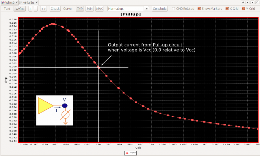
- Z_PU: impedance of PU circuit at the reference voltage;
- Z_PD: impedance of PD circuit at the reference voltage;
- Z_PU_MM in %: impedance mismatch of PU circuit at some tolerance above and below the reference voltage. It’s like linearity measurement between VOH and VOL for PU circuit.
- Z_PD_MM in %: impedance mismatch of PD circuit at some tolerance above and below the reference voltage. It’s like linearity measurement between VOH and VOL for PD circuit.
- Z_RTT: This is the impedance representing aforementioned termination resistor(s);
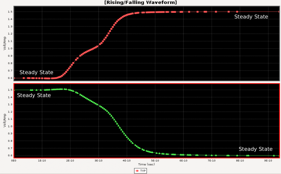
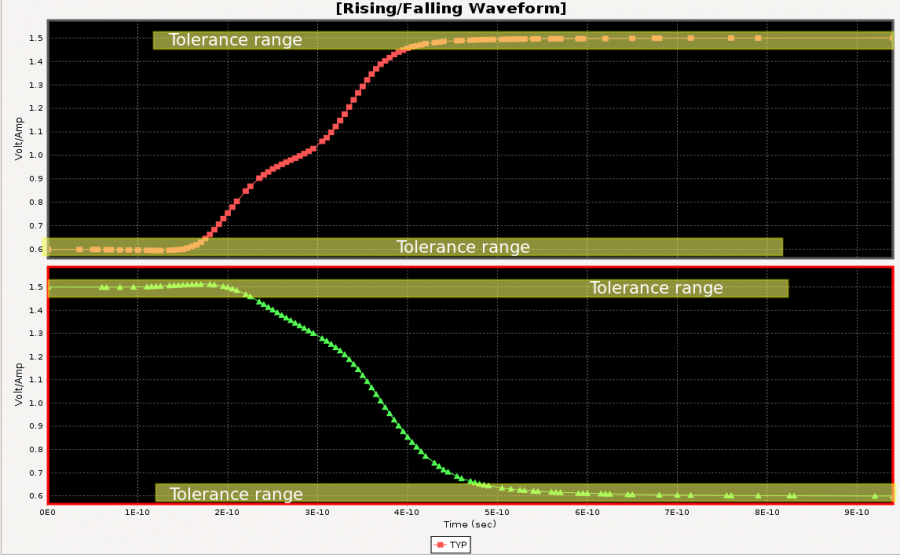
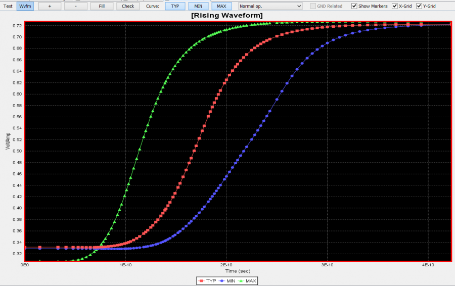
- RT: time duration between 20%~80% of voltage swing during rising transition;
- FT: time duration between 20%~80% of voltage swing during falling transition;
- FREQ: maximum operable frequency without buffer being overclocked.
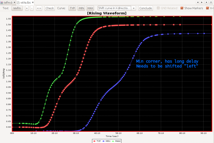
Note that some people may use Tco, the propagation delay between buffer output and its digital input, as parameters as well. It’s our believe that these Tco parameters are not too meaningful. We mentioned in earlier posts that a modeling engineer or circuit simulator may sacrifice the leading steady state portion of the VT curve in order to capture most portion of the transition behavior in high speed design. Tco is not kept in the model in these case. Also, SI engineers often look at the quality with eye plot, which is folded signal of different bits. There is no eye impact (eye height or eye width) by the Tco parameters as the full response to the input bit sequence has been shifted with the same amount of time, difference of true Tco and model presented Tco value.
With these parameters, one may generate a summarized table when given a library of IBIS models and will be able to find the best candidate for driving signal down the communication channel.
Generate spec. model:
Using these spec. parameters, we may further define and generate IBIS model for our early stage signal study. We can do the sweep on some of these parameters and generate artificial IBIS model accordingly. With this model for simulation and the analysis results, an SI engineer may provide this as a feedback to the circuit designer for desired performance. As a modern buffer is usually controlled by many “legs”, a circuit design should be able to find certain combinations of these “ON” lags to satisfy the system engineer’s need, or use the feedback as a guideline in fine tuning their buffer control circuit.
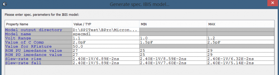
SPISim BPro’s Spec. model generation
With this concept, SPISim BPro takes one step further to support spec model generation, as shown in screenshot above. User can enter the appropriate settings and the corresponding IBIS model, with rising and falling waveform table included, will be generated instantaneously without any simulation. One then may use the manual waveform editor as needed to fine tune the transition waveform shape based on this spec. model.
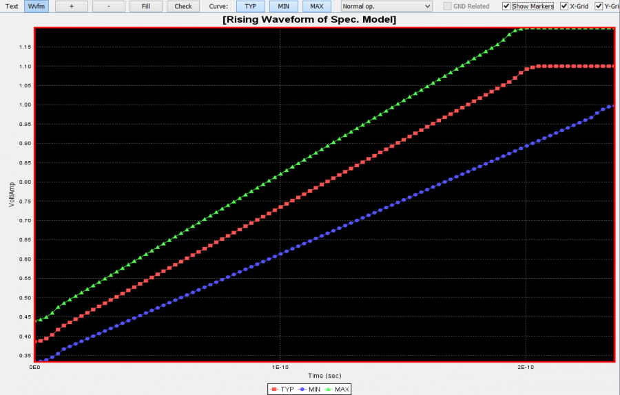
BPro generated spec model will have smooth transitions.