
In this post, we would like to talk about debugging IBIS model and performance tuning. As discussed in previous posts, one of the first and important steps to make sure IBIS model generated from simulation data is valid is to run with IBIS committee released golden parser. Often times, the parser will output the following errors or warning messages for models with suspicious qualities:
- DC mismatch: mismatch between VT’s steady state and IV data;
- Non-monotonic data points in I/V curve;
- Extreme currents in IV data.
We are going to discuss these in more details below. For performance tuning, we are going to talk about buffer overclocking and the associated accuracy concerns. This is important because it will make sure your buffer will run at desired speed or lower without producing erroneous response. We also briefly talk about solution implemented in our SPIBPro modeling tool to meet the overclocking challenges.
DC mismatch:
One of the most troublesome messages output by golden parser is the DC mismatch warnings/errors:
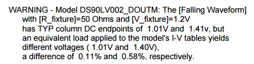
When the mismatch percentage is small, what’s visible to modeling engineer is that their IBIS model will not produce exactly same dc steady state voltages comparing to those from original transistor buffer design. The usual remedy often is to go back and check the IV simulation setup and biasing conditions then regenerate model and check again. The last resort is to use editor like those in our BPro to manually adjust the data points mostly in IV table such that the DC mismatch will alleviate or even go away. To know how to fix this problem, we need to explain what this message means:
Steady state at the beginning and ending of the VT waveform
In the figure above, the beginning and ending points of each VT table, be it rising waveform or falling waveform, are assume to have reached steady state. These two steady states are taken by the IBIS parser to perform check for DC mismatch. During steady state, voltages are assumed to stay the same and the time point is irrelevant. Since each VT table comes with test fixture information, one may compute load line current with these two voltage points and the given fixture info.
DC mismatch is due to mismatched steady state and IV data point
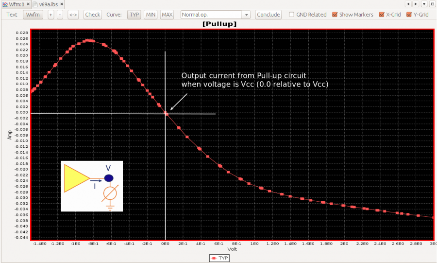
In the figure above, we depict a buffer output to a test load setup, represented by variable R fixture to V fixture to ground in this case at the lower left. The load line current I is V / R. That is, when the nodal voltage at pad is V, the output current I can be computed as:
- I_LoadLine = (V_Pad – V_Fixture) / R_Fixture
Now this current is contributed by those pull-up (PU, PC) and pull-down (PD, GC) circuits. At logic high output state, we may assume PD are fully off (current contribution is 0.0), so current at this point is from PU mainly minus small reverse bias current from PC and GC. When looking at the PU’s IV table, we can find this V_Pad, minus Vcc (as PU’s voltage is “Vcc relative”), find out the I_PU for this voltage point. We can then find I_PC and I_GC similarly using PC and GC table if they are present (remember PC is also “Vcc relative”). Finally I_Out is I_PU – I_PC – I_GC. that is, based on these IV tables, this buffer will output current equivalent to I_Out. DC Mismatch means I_LoadLine is not equal to I_Out. That is, the output current computed from the VT’s ending points is not same as that computed based on the given IV tables.
What we just described is for logic high situation, i.e. ending point or rising waveform or starting point of falling waveform. For logic low output situation, the process is similar, only that in this case, PU is assumed to be fully “OFF” so most of the current drawn is from the PD branch.
Knowing the causes of this errors, then the approaches to fix become apparent. Either one may need to adjust (manually or check and re-simulate to generate) IV table, or need to check whether the VT wavform make sense or not. Our experience show that 90% of the case, IV simulation is not done correctly, either because bias condition was not setup properly, or the “pseudo-transient” methods change voltage too fast such that the current measured is not true “steady state” current.
Non-Monotonic Points in I/V data:
This messages means the table is non-monotonic, meaning the sign of its first derivative changes. Our experience shows that these types of warnings are usually OK to ignore. However, strong non-monotonicity may cause simulator trouble to find solutions around that region, thus cause non-convergence issue.
Often time these troubling points are in the non-active region of the device and can be “smooth” out easily by deleting offending or adding points. It should also be noted that some devices do exhibit non-monotonic behavior, so artificially removing them either to make it more appearing visually or to avoid parser warnings may cause concern of the model recipients about accuracy of this model, if they are also knowledgeable about this type of buffer design.
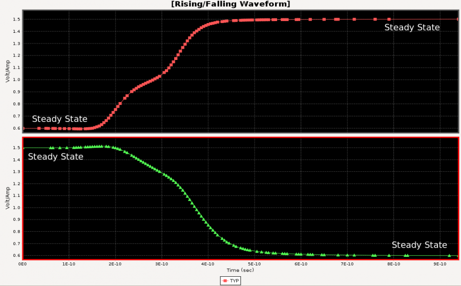
Extreme current in IV data:

This happens most common to power clamp (PC) and ground clamp (GC) data table. However, since PC/GC currents can’t be removed and must be subtracted from the PU/PD (pull-up/pull-down) current during modeling, it may also means that PC/GC currents are not captured properly in PU/PD such that after subtraction, PU/PD data table shows signs of “break down” current like those in the PC/GC.
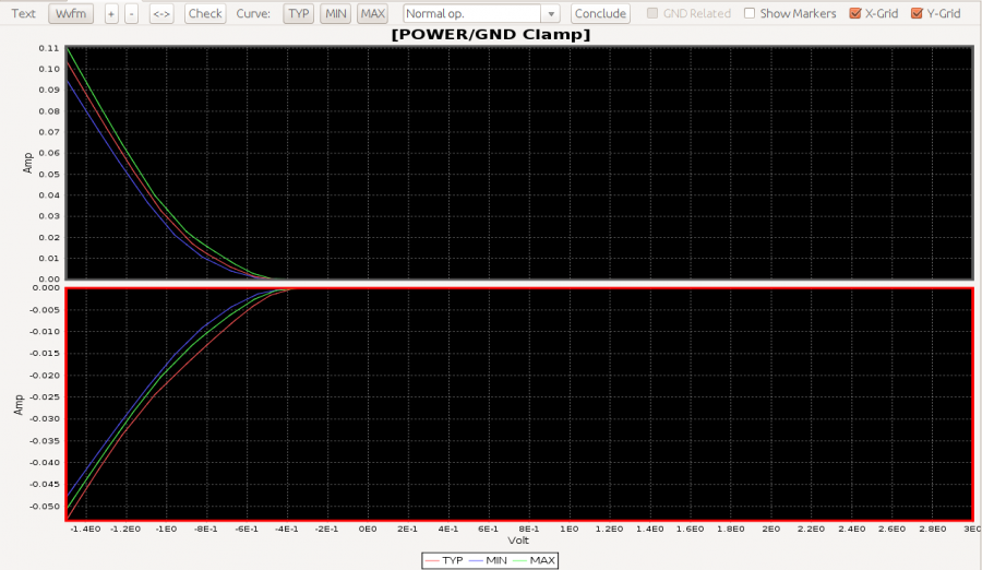
The picture above shown typical PC/GC curve. As one can see, most of the time (in normal buffer operating region), the curve is relative flat and value is small. This is in reverse bias region and leakage current is small. However, due to the -Vcc ~ 2Vcc requirement of the IBIS modeling to account for total reflection. the ESD circuit may well march into the “break down” region and have exponential like current output or drawn from the pad. It is in this area which may cause extreme current warning.
Since the buffer operate in ESD’s reverse bias region mostly, the approach to fix this can be simple, albeit a little artificial. One may find the data point at least 1 volt beyond points when ESD starts to breakdown and use these two points for extrapolation. This way the exponential like curves are converted to linear with still sufficient current output/drawn to allow ESD circuit, represented by PC/GC, to protect the circuits connecting to the buffer’s output.
Buffer Overclocking:
Each set of rising and falling waveform combined to form a complete period, T. The maximum frequency a circuit simulator can operate this buffer thus is FMax = 1 / T. That is, the longer the T is, the lower speed buffer can operate without letting simulator sacrificing some of model’s original data.
When a buffer is operated at a higher frequency than its models allows, FMax, this buffer is being overclocked. Overclocked buffer may produce inconsistency issue, as explained below.
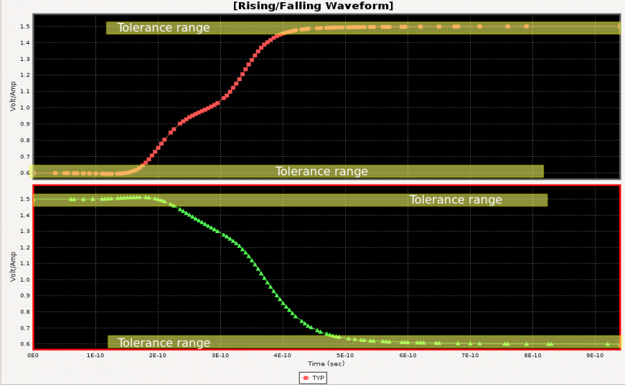
The figure above shows a typical untrimmed VT simulation data or IBIS model VT waveform. One will find that the steady state portion occupies great portion of the data points. So if we set a tolerance range around these steady states and trim to remove those data points, we may end up with a much shorter duration of the data table which still captures the majority of the transition informatino, yet can be operated at a much higher frequency.
Normally this type of the “trimming” can be done by the circuit simulator automatically. However, being a modeling developer, you would not want to limit your user choice of simulators. Since IBIS spec does not give a clear messages how a circuit simulator should trim the data (e.g, trim from back or from the beginning, with how much tolerance?), one may often find simulation results inconsistent when different simulators are used on the same IBIS model, particular at a higher frequency.
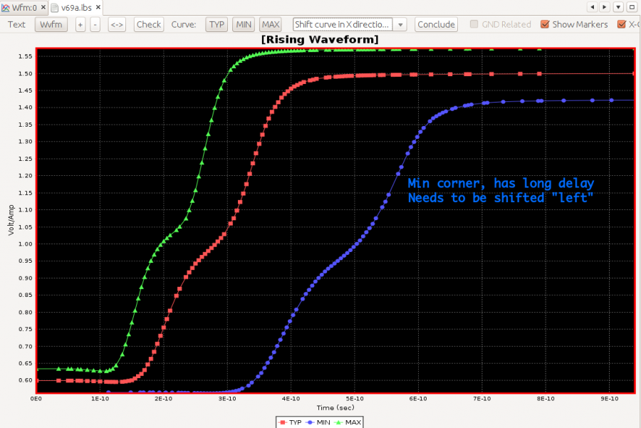
MIN corner has much longer delay
Another example of source of overclocking is shown above. In this case, the min corner waveform, represented in blue, has much longer delay than the other two corners. Since the IBIS spec. requires that all TYP/MIN/MAX corner should share the same set of X-data (time), the MIN corner will then be easily overclocked or even won’t have enough transition information captured in the produced IBIS model.
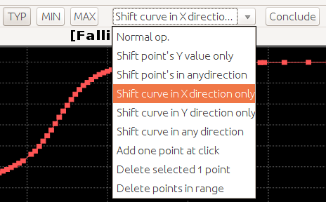
To address this overclocking issue, SPISim propose letting user gain finer control of the trimming behavior. Also let tool take care of the tuning after trimming is done to avoid aforementioned DC mismatch issue. Another handy solution is to use editor provided by BPro to allow certain degrees of manual editing easily.
SPISim BPro’s manual tuning capabilities
Note that besides the voltage portion we have discussed so far, power aware IBIS 5.0 model also present another challenge: The composite current, which contains crow-bar current as well, usually starts being active even when output voltage is still steady. As a result, simulator can’t trim out the leading steady state voltage because doing so, will sacrifice the current information presented in the model. We will discuss this problem and propose solution further in future post.