IBIS-AMI: Study of DDR Asymmetric Rt/Ft in Existing IBIS-AMI Flow

[This blog post is written in preparation for the presentation of the same title to be given at the 2019 DesignCon IBIS Summit. Presentation slides and audio recording are linked at the bottom of this post.]

This paper is written by both Wei-hsing Huang (principle consultant at SPISim USA) and Wei-kai Shih, who is Tokyo based.

Motivation:

Here in US, one of IBIS committee’s working groups, IBIS-ATM (advanced technology modeling) has regular meeting on Tue. I try to call-in whenever possible to gain insights on upcoming modeling trends. During mid 2018, DDR5 related topics were brought up: Existing AMI reference flow described in the spec. focuses on differential or SERDES. For example, the stimulus waveform is from -0.5 to 0.5 and/or a single impulse response is used for analysis, thus assuming symmetric rise time (Rt) and fall time (Ft) mostly. Whether this reference flow can be applied to DDR, which may have asymmetric Rt/Ft and single-ended like DQ, is the center of discussion. Different EDA companies in this work group have different opinions. Some think the flow can be used directly with minimal change while others think the flow has fundamental shortcomings for DDR. Thing about IBIS spec. change is that whoever think the current version has deficiencies needs to write a “buffer issue resolution document (BIRD)”. Doing so will inevitably disclose some of the trade secrets or expose shortcoming of the the tool. As a result, while there are companies which think change may be needed, no flow change have been proposed at this point. As a model maker, I wonder then how existing flow can be applied to DDR without major change? Thus this study is to demonstrate “one” possible implementation. Existing EDA companies may have more sophisticated algorithms/implementations to support this asymmetric condition, but the existence of “one” such possible flow may convince model makers that it’s time to think about how DDR AMI may be implemented rather than waiting for the unlikely spec. change.

AMI_Init:

There are both “statistical” and “bit-by-bit” flows in channel analysis. In either case, the first step an EDA tool will do before calling AMI model is “channel calibration”. According to the spec. the impulse response of the channel, which includes analog buffer, is obtained here. For a SERDES design which has no asymmetric Rt/Ft issue, this impulse is then sent to TX AMI followed by RX AMI, resulting impulse response is then calculated using probability density function (PDF), integrated to be cumulative density function (CDF), then obtain bathtub plots etc.

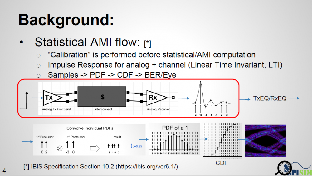
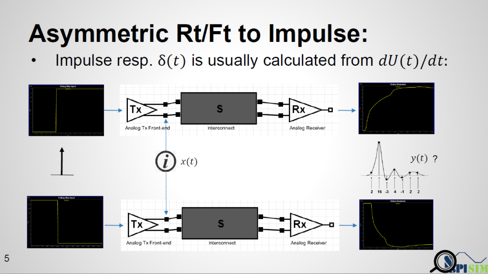
The textbook definition of an impulse response is from a “delta response” input which happens at the infinite small time step. In real situation, there is no such thing as an “infinite small time step”. The minimal step used by a simulator is a “time step” which is usually 1ps or more. Buffer will not toggle from low to high back to low in a single time step. So in reality, simulator often uses step response then take derivative to get impulse response. Now the problem comes: for an analog channel with asymmetric Rt/Ft, these two step response (ignoring the sign) are different. That means we will have two different impulse response, then which one should be send to AMI models? A note here up front is that it’s EDA tool which sets up the calibration, so it has any nodal information, such as pad of Tx and Rx analog buffer, if needed.

Asymmetric Rt/Ft:

One may think that there is no such limitation that an AMI model can only be called once. So theoretically, a simulator can run analysis flow twice… impulse calculated from rising step response is used for the first time and the one from falling step response is used for the second time. However, not only is this not efficient, a model may not be implemented properly such that calling AMI_Init again right after AMI_Close may cause crash if it’s in the same process and model pointer was not released completely. Thus doing so may hamper a simulator’s robustness.

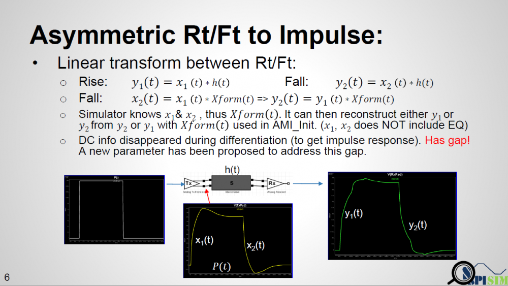
As depicted in the picture above… if a simulator uses a long UI pulse to calibrate the channel, then both rising and falling step response are included in one simulation. Now let the data captured at Tx analog pad as X1 and X2 for rising and falling portion respectively, the data captured at Rx analog pad Y1 and Y2 will be X1 and X2 convolved with interconnect’s transfer function, which is LTI. If we derive a Xform(t) which is transfer function between X1 and X2, then that Xform(t) should also be able to transform between Y1 and Y2.  That means if a simulator can calculate Xform(t) it self, then regardless the impulse response it sent to AMI models is calculated from rising or falling step response, it can always “reconstruct” the result from the other type of impulse response using this Xform(t) function.

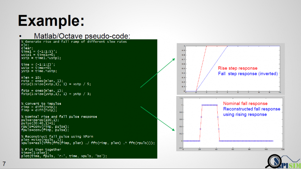
To prove this concept, we have written a simple matlab script taking step inputs of different slew rate, say inp1 and inp2. It calculates the Xform(t) function from both inputs and then reconstruct the response out2′ from out1. When overlaying nominal output out2 and reconstructed out2′ together, we can see that they match very well, thus prove the concept.

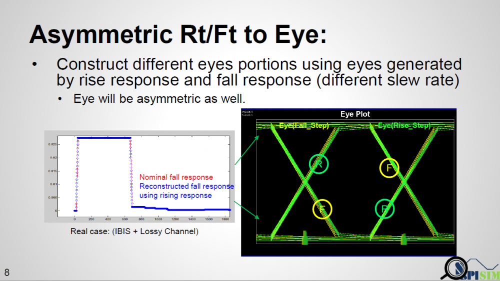
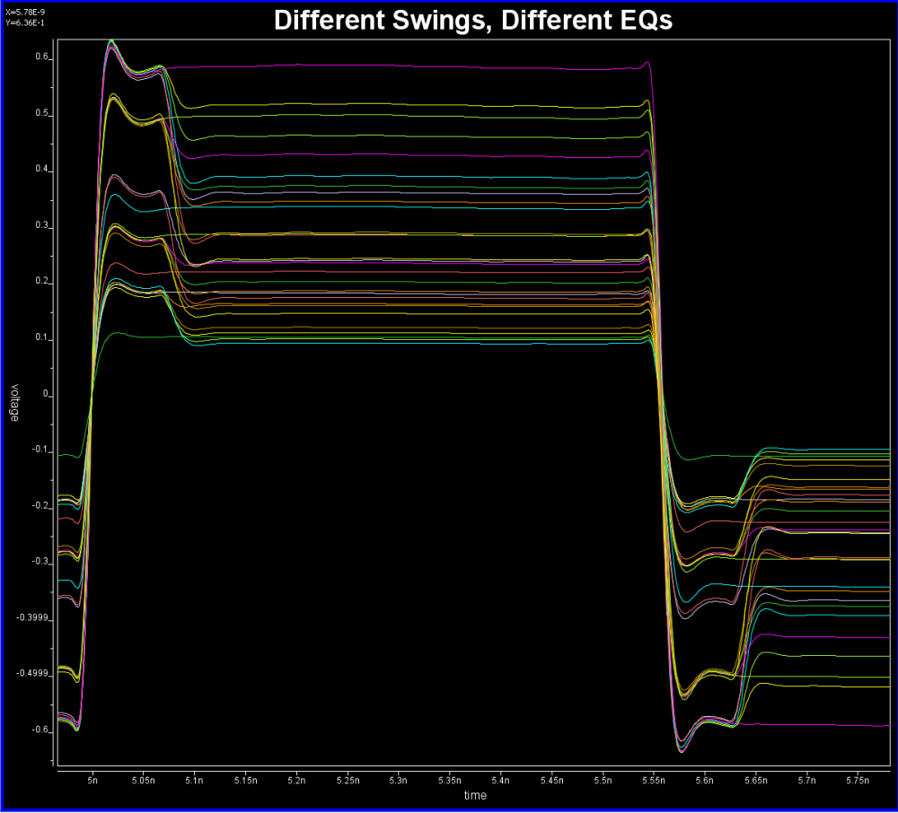
Once we have response from both different slew rates, we can construct their respective eyes then use each one’s different portion to construct a synthesized eye. Such eye will not be symmetric like that calculated from SERDES.

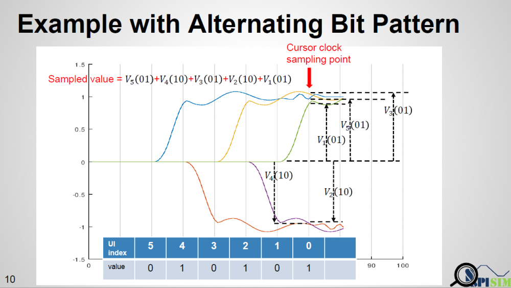
When calculating PDF for asymmetric case, one may also need to consider the precedent bit’s value and use a tree like structure to keep track of possible bit sequence. For example, for a typical SERDES bit sequence, if encoding is not considered, each bit will have 50% one and 50% zero. PDF is constructed based on that assumption. But in an asymmetric case, if the data used at the cursor is from rising response, then the cursor bit must be 1 while (cursor – 1) must be zero. If (cursor – 2) is 1 again, then the tail of falling response at (cursor – 1) will be superimposed to the cursor data. That is, we can’t treat each bit to have same 50% probability when constructing PDF. It’s not a binomial distribution as each occurrence is not independent. A simulator may need to determine the maximum bit length to keep track of first, then based on that depth to form tree-like sequence which leads to the rising or falling steps at the cursor location. Finally use superimpose to construct the overall response.

AMI_GetWave:

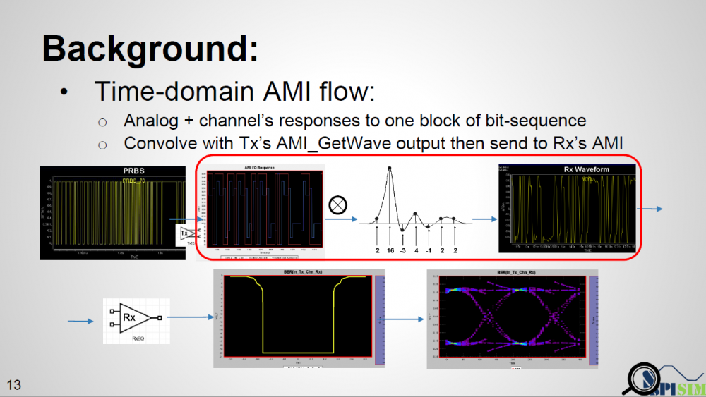
According to the reference flow for the bit-by-bit case: equalized Tx output from digital bit sequence is converted with channel’s impulse response. The resulting waveform is then sent to Rx EQ before getting final results. Either Tx EQ or Rx EQ or both may not be LTI so usage of aforementioned Xform(t) is not applicable.

As a fruit of thought… the spec. only mentions that in a bit-by-bit mode, the output of Tx AMI model is equalized digital sequence, while input to the Rx EQ must be the channel response from that sequence, then are there other ways to get such response to Rx yet with different Rt/Ft considered?

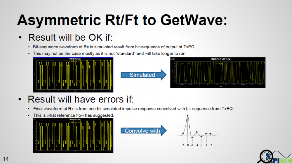
One example is like shown in top half of the picture above. If a simulator takes that equalized digital input and “simulate” to get final response, then this “simulation process” should have taken different Rt/Ft into account and has valid results. However, this process will be slow and I don’t think any simulator is doing it this way. Furthermore, the spec. specifically say it needs to “convolve” with impulse response. First of all, this impulse can be from rising or falling. Secondly, even we decide to decovolve with input first (thus has sequences of different delta response) then convolve with pulse response (i.e. one simulated UI), will there be any issue?

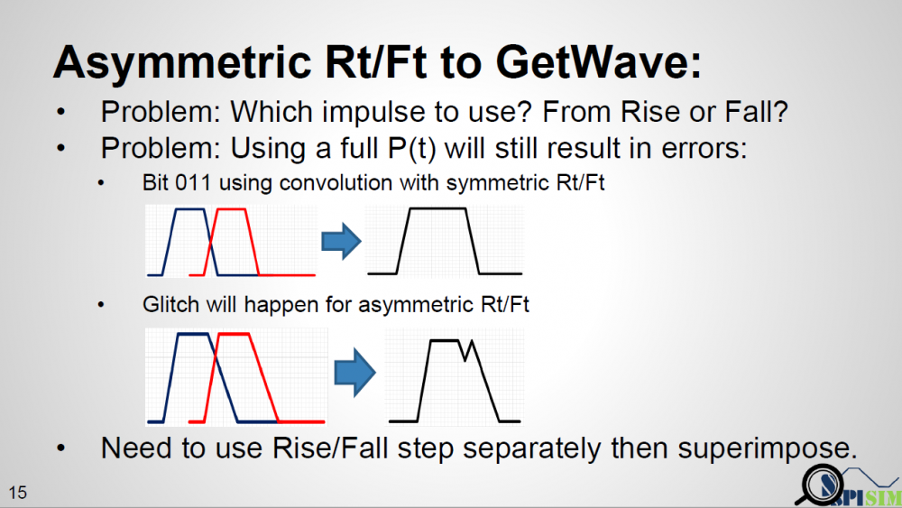
From the plot above…  we can see that when a pulse has different rising and falling slew rate, using superimpose to construct 011… will find “glitches” at the trailing high state portion. The severity of this “glitches” depends on how much difference the Rt/Ft is. So using a pulse response here will still not work.

A simple matlab script has also been written to demonstrate occurrence of such “glitches”. This proves that not only using an impulse response to convolve with Tx EQ’s output is problematic, even using a full simulated pulse (which has asymmetric Rt/Ft’s effect) to convolve delta sequences (this delta sequence is original TX EQ’s output deconvolve with one digital bit) will still be problematic. Glitches will happen for consecutive ones or zeros due to the mismatches of Rt and Ft. Thus one must use rise step and fall step response instead when doing such kind of convolution.

Summary:

In this presentation, we discussed how existing AMI flow may be applied to asymmetric Rt/Ft such as those often seen in DDR case. A “smarter” EDA tool should be able to handle this situation without changing on spec.’s reference flow. When a channel analysis is performed in a “statistical” flow, an EDA tool can obtain waveform data at both Tx and Rx analog buffer’s pads during calibration process. Such data can be used to construct a transform function, XForm(t). With this function, impulse response through EQ can be reconstructed and thus built an asymmetric eye. Tree structure may be needed to keep track of possible bit combinations. In a “bit-by-bit” flow, the current spec. may be too specific as it forces to use convolution of TX EQ’s output with channel’s impulse response before sending to RX EQ. Such direct convolution may be problematic. A “smarter” simulator may calculate it using different method without changing data output from TX EQ and input to the RX EQ. Step response should be used as different Rt/Ft will cause “glitches” when consecutive ones/zeros are present if convolution method is used.

Links:

Presentation: [HERE] (http://www.spisim.com/support/paperetc/20180202_DesignConSummit_SPISim.pdf)

Audio recording (English): [HERE]

IBIS-AMI: An end-to-end AMI modeling flow

In previous post, I mentioned about the “IBIS cook-book” as a good reference for the analog portion of the buffer modeling. Unfortunately, when it comes to the equalization part, i.e. AMI, there is no similar counterpart AFAIK. For the AMI modeling, the EQ algorithms need to be realized with algorithms/procedures implemented as spec. compliant APIs and written in C language. These functions then need to be compiled as a dynamic library in either dynamic link libraries (.dll on windows) or “shared objects (.so on linux-like). Different compiler and build tool has different ways to create such files. So it’s fair to say that many of these aspects are actually in the computer science/programming domains which are outside the electrical or modeling scopes. It is unlikely to have a document to detail all these processes step-by-step.

In this post, instead of writing those “programming” details, I would like to give a high-level overview about what different steps of the AMI modeling process are… from end to end.  Briefly, they can be arranged in the following steps based on execution order:

  1. Analog modeling
  2. Prepare collateral
  3. Define architecture
  4. Create models
  5. Model validation
  6. Channel correlation
  7. Documentation

The following sections will describe each part in details.

Analog modeling:

Believe it or not, the first step of AMI modeling is to create proper IBIS models… i.e. its analog portion. This is particular true if circuit being modeled belongs to TX. A TX AMI model is equalizing signals which includes its own analog buffer’s effect measured at the TX pad. So if there is no channel (pass-through) and it’s under nominal loading condition, the analog response of the TX will be the signals to be equalized. That is to say, without knowing what will be equalized (i.e. what the model’s analog behavior is), one can’t calculate the TX AMI model’s EQ parameters.

Take the plot above as an example. This is a FFE EQ circuit. The flat lines indicated by two yellow arrows are different de-emphasis settings, thus controlled by AMI. However, the rising/falling slew rate, wave shape and dc levels etc as circled in red are all analog behaviors. Thus an accurate IBIS model must be created first to establish the base lines for equalization. Recently, BIRD 194 has been proposed to use touch-stone file in lieu of an IBIS model… still the analog model must be there.

For a RX circuit, it may be easier as an input buffer is usually just a ESD clamp or terminator. Thus it doesn’t take much effort to create the IBIS model. Interested people may see my previous posts regarding various IBIS modeling topics.

Prepare collateral:

AMI’s data can be obtained from different sources: circuit simulation, lab/silicon measurement or data sheet. For simulation case, simulation must be done and the resulting waveform’s performance needs to be extracted. These values will serve as a “design targets” based on whitch AMI model’s parameters are being tuned.

For example, this is a typical TX waveform and measured data:

Various curves have been “lined-up” for easy post-processing. Using our VPro, we batch measured the value at the 5.3ns for different curves and created a table:
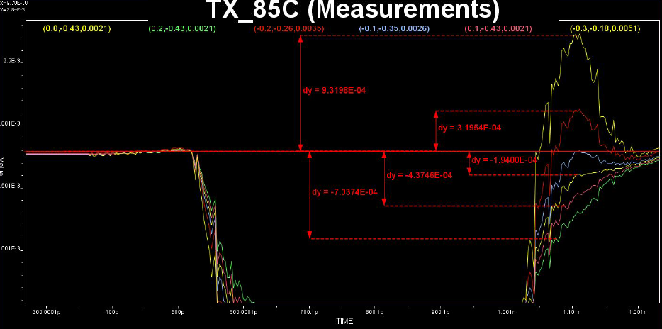
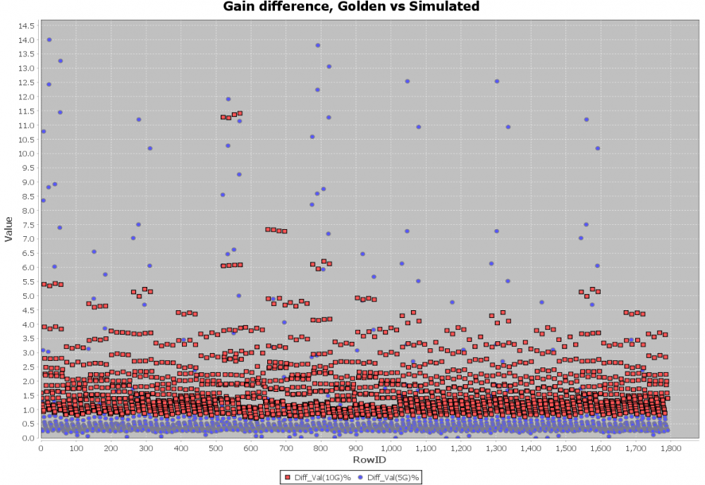
Similarly, data collected from measurement needs to be quantified. This may be done manually and maybe labor intensive as the noise is usually there:

Some of the circuits may have response is in frequency domain. In this case, various points (DC, fundamental freq. 2X fundamental etc) needs to be measured like above.

If it’s from data sheet, then the values are already there yet there may be different ways to realize such performance. For example, equations of different zeros and poles locations may all have same DC gain or gain at particular frequencies, so which one to pick may depending on other factors.

Define architecture:

Based on the collateral and the data sheet, the modeler needs to determine how the AMI models will be built. Usually it should reflect the IC’s design functions so there are not much ambiguity here. For example, if the Rx circuit has DFE/CDR functions, then the AMI models must also contain such modules. On the other hand, some data my be represented in different ways and proper judgement needs to be made. Take this waveform as an example:

It’s already very obvious that it has a FFE with one post-tap. However, since the analog behavior needs to be represented by an IBIS model, then one needs to decide how these different behaviors, boxed in different colors, should be modeled. They can be constructed with several different IBIS models or a single IBIS model yet with some “scaling” block included so that IBIS of similar wave shapes can be squeezed or stretched. For a repeater, oftentimes people only care about what goes into and what comes out of this AMI model. The abilities to “probe” signals between a repeater’s RX and TX may be limited by the capabilities of simulator used. As a result, a modeler may have freedom determining which functions go into Rx and which go to Tx. In some cases, same model yet with different architecture needs to be created to meet different usage scenarios. An example has been discussed in our previous post [HERE]

Create models:

Once architecture is defined, next step is the actual C/C++ implementation. This is where programming part starts. Ideally, building blocks from previous projects are there already or will be created as a module so that they can be reused in the future. Multiple instance of the same models may be loaded together in some cases so the usage of “static” variables or function need to be very careful. Good programming practice comes into play here. I have seen models only work with certain bit-rate and 32 samples per UI. That indicates the model is “hard-coded”… it does not have codes to up-sample or down-sample the data based on the sampling-interval passed in from the API function. Accompanied with writing model’s C codes are unit testing, source revision control, compilations and dependencies check etc. The last one is particular important on linux as if your model relies on some external libraries and it is not linked statically, the same model running fine on developer’s machine will not even pass golden checker at user’s end…. because the library is not available there. Typically one will need to prepare several machines, virtual or not, which are “fresh” from OS installation and are the oldest “distros” one is willing to support. All these are typical software development process being applied toward this AMI modeling scope.

After the binary .dll/.so files are generated, then next step is to assemble a proper .ami files. Depending on parameter types (integer, values, corners etc), different flavors of syntax are available to create such file. In addition, different EDA simulators has different ways to present the parameter selections to its end user. So one may need to choose best syntax so that choices of parameter values will always be selected properly in targeted simulators. For example, if one already select TYP/MIN/MAX corner for the IBIS model, he/she should not have to do so again for the AMI part. It doesn’t make sense at all if a MIN AMI model will be used with MAX corner IBIS model… the corner should be “synchronized”.

Once the model is ready, next step is to tune the parameters so that each of the performance target will be matched. Some interface, such as PCIe, has pre-defined FFE tap weights so there are no ambiguities. In most cases, one need to find the parameter’s values to match measured or simulated performance. Such tasks is very tedious and error prone if doing manually and process like our “AutoTune” will come very handy:

Basically, our tool let user specify matching target and tool will use bisection algorithm to find the tap values. Hundred of cases can be “tuned” in a matter of minutes. In some other cases, grid search may be needed.

Model validation:

Just like traditional IBIS, the first step of model validation is to run it through golden checker. However, one needs to do so on different platforms:

The golden checker didn’t start checking the included AMI binary models until quite recently. Basically it loads the .ibs file, identifies models with AMI functions, then check the .ami file syntax. Finally, the checker will load the associated .dll/.so files. Due to the fact that different OS platform loads binary files differently, that means certain models (e.g. .dll) can only be checked on associated platform (e.g. Windows). That’s why one needs to perform the same check on different platforms to make sure they are all successful. Library dependencies or platform issues can be identified quickly here. However, the golden checker will not drive the binary file. So the functional checks described in next paragraph will be next step.

Typically, an AMI model have several parameters. To validate a model thoroughly, all combinations of these parameters values need to be exercised. We can “parameterize” settings in a .ami file like below:

Here, pattern like %VARIABLE_NAME% is used to create a .ami template. Then our SPIMPro can be used to generate all combinations of possible parameter values and create as a table. There can usually be hundreds or even thousands cases. Similar to the process described in “Systematic approach mentioned in my previous post”, we can then generate corresponding .ami files for all these cases. So there will be hundreds or thousands of them! Next step is to be able to “drive” them and obtain single model’s performance. Depending on the EDA tools, most of them either do not have automation capability to do this in batch mode or may require further programming. In our case, our SPIMPro and SPIVPro have built-in functions to support this sweeping flow in batch mode all in the same environment. SPISimAMI model driver is used extensively here! Once each case’s simulation is done, again one needs to extract the performance then compare with those obtained from raw data and make delta comparison.

A scattering plot like below will quickly indicate which AMI parameter combinations may not work properly in newly created AMI models. In this case, one needs to go back to the modeling stage to check the codes then do this sweep validation all over again.

Channel correlation:

The model validation mentioned in previous section is only for a single model, not the full channel. So one still needs to pick several full channels set-up to fully qualify the models. A caveat of the channel analysis is that it only shows time domain data regardless the flow is “statistical” or “bit-by-bit”, that means it is often not easy to qualify frequency domain component such as CTLE. In this case, a corresponding s-parameter whose Sdd12 (differential input to differential output) is represented by this CTLE AMI settings can be used for an apple-to-apple comparison, like schematic shown below:

Another required step here is to test with different EDA vendor’s tool. This presents another challenge because channel simulator is usually pricey and it’s rarely the case that one company will have all of them (e.g. ADS, HyperLynx, SystemSI, QCD and HSpice etc). Different EDA tools does invoke AMI models differently… for example, some simulator passes absolute path for DLL_Path reserved parameter while others only sent relative path. So without going through this step, it’s difficult to predict what a model will behave on different tools.

Documentation:

Once all these are done, the final step is of course to create an AMI model usage guide together with some sample set-ups. Usually it will starts with IBIS model’s pin model associations and some performance chart, followed by descriptions of different AMI parameters’ meaning and mapping to the data sheet. One may also add extra info. such as alternatives if the user’s EDA tool does not support newer keyword such as Dll_Path, Dll_ID or Supporting_Files etc. Waveform comparison between original data (silicon measurement vs AMI results) should also be included. Finally it will be beneficial to provide instructions on how an example channel using this model can be set-up in popular EDA tools such as ADS, HyperLynx or HSpice.

Summary:

There you have it.. the end-to-end AMI modeling process without touching programming details! Both AMI API and programming languages are moving targets as they both evolve with time. Thus one must continue honing skills and techniques involved to be able to deliver good quality models efficiently and quickly. This is a task which requires disciplines and experience of different domains. After sharing these with you readers, do you still want to do it yourself? 🙂 Happy modeling!

A quick and easy IBIS modeling flow

For engineers who are new to IBIS modeling, the “IBIS CookBook” [LINK HERE] is a very good reference document to get started. The latest version, V4.0, was created back in 2005. While most of the documented extraction procedures still hold true to this date, some of them may be tedious or even ambiguous in terms of executions. This is particular true for processes mentioned in Chapter 4, differential buffer modeling. Further more, most recent IBIS summit presentations focus on “new and hot” topics like IBIS-AMI modeling methodologies and not many are for the traditional IBIS. In this post, I would like to first review these “formal” process, dive into how each modeling table is extracted and used in simulation, then propose a “quick and easy” method particular for differential buffer. I will then summarize with and this approach’s pros and cons.

IBIS model components:

The most basic IBIS building block, as defined in Spec. Version 3.2, is shown above. Typically at least six tables will be included in an output type buffer. They are IV (Pull-up, Pull-down) and Vt( Rising and falling) under two different test load conditions. Additional clamp IV table (Power and Ground clamp) may be added for input type buffer. After Spec version V5.1, Six additional IT tables for ISSO_PU/PD/Composite currents have also been added to address PDN effects. To create an IBIS model, the data extraction processes start with exciting particular portion of the buffer so that measured data can be post-processed to formulate as a spec-compatible table format. Because a model also has TYP/MIN/MAX skews, so the number of simulations are basically the aforementioned number of tables times three. That is, for a most basic IBIS modeling, one may need to simulate at least eighteen cases (or simulation  “decks”).

To explain a little bit more regarding blocks untouched by proposed new method, I list them in the bullets below:

  • Package/Pin parasitics: IBIS cookbook and normal modeling flow do not mention about this part. Usually a buffer package’s model is extracted using tools such as HFSS or Q3d into a form of S-parameters or equivalent broad-band spice model. An IBIS model can use a lumped R+L+C structure to describe pin specific or package (apply to all pins) specific parasitics. Alternatively, an IBIS model can also use a more detailed tree structure package model shown below for non-lumped structure. Regardless, it’s HFSS or Q3D’s task to convert such extracted S-parameter or multi-terminal sub-circuit into these simple lumped RLC values or tree structures to be included in an IBIS file. It’s a separated process and not discussed here as a part of the buffer modeling.

  • C_Comp: At the very beginning, there is only a C_Comp value between pad and ground and it is used to describe frequency dependent behavior besides the parasitics. Later on, tool like HSpice introduces extra simulation syntax to split this single C_Comp value into branches between pad and various power terminals for better accuracy. Even later, this type of syntax was adopted as part of the IBIS spec. Still, user may only find how a single C_Comp value is computed in most materials. Briefly speaking, they can be calculated using time-domain method based on RC charging/discharging time constant or freq-domain method based on the imaginary current at a particular frequency. How to split this single value into several ones to match the frequency plot best remains an art (i.e. not standardize). In addition, the value C_Comp is not visible during modeling… their effects are only shown when there are reflections back from the other end due to impedance mismatch. What we have found is that usually an IC designer has a better idea about how this value should be and the aforementioned time/frequency domain calculation method may not produce an accurate estimate.

  • Clamp current: Power/Ground clamp currents and Pull-up/Pull-down currents are both IV based (i.e. dc steady state). So they are combined for load-line analysis during simulation. The difference between Pull-up/Pull-down and Clamp is that the latter one (i.e. Clamp) can’t be turned-off. So its effect is always there even when we are extracting IV for Pull-up/Pull-down structures. Thus to avoid “double-counting”, the post-processing stage needs to remove the clamp current from pull-up/pull-down currents first before putting them into separated table. To simplify the situation… particular for an output differential buffer, we may just use IV data even though this is an IO buffer.
  • IT current: These are different dc or transient based sweep in order to obtain buffer’s drawing current when power or ground are not “ideal”. This is important in DDR case when the DQ is single ended and it’s subjective to PDN’s noise. For differential application like SERDES, PDN’s effects are usually present at both the P and N terminals and will cancel with each other. Thus their extraction may be skipped for a differential buffer mostly. One may also note that the IT extraction of composite current is “synchronized” with VT extraction of rising/falling waveform so these current data are extracted with additional “probes” rather than separated simulation.

Full IBIS modeling flow:

The process suggested in IBIS’s cookbook can be summarized as the following steps. They are also implemented in our “Full IBIS modeling flow” within SPIBPro:

  • 0, Collect design data and collateral: A modeler needs to gather PVT (process, voltage, temperature) data, silicon design, buffer terminals’ definitions and bias conditions etc. A buffer may have several tuning “legs” and bit-set settings so a modeler needs to determine which will be used for TYP, MIN and MAX corners.
  • 1, Prepare working space: Create a working space on the disk.
  • 2, Generate simulation inputs: Generate simulation “decks” to excite different block of the buffer…one at a time. So one will have eighteen or more decks at the end of this stage waiting to be simulated.
  • 3, Perform simulations: Perform simulation either sequentially on a local machine or with a simulation “farm”. Double check the results and make sure they make sense, otherwise, go back to step 0 to see which settings may be incorrect or missing.
  • 4, Generate IBIS model: Post-process the simulation data and generate IBIS model. This is usually done by the tool like ours as manual process is tedious and error prone.
  • 5, Syntax check: First quality check of an IBIS model is that it must pass the golden checker. The check here is mostly syntax-wise though there are also basic behavior check such as monotonicity or DC mismatch etc.
  • 6, Validate IBIS model: A formal validation for an IBIS model is to hook-up test load and make sure they produce correlated results comparing to those from silicon at the end of step 3 above.
  • 7, Performance report: The modeler needs to extract the performance such as PU/PD impedance values and slew rate etc. for documentation purpose and check against the spec. or data sheet.

Full step-by-step modeling flow in SPIBPro

Data extraction for a single-ended buffer:

For a single-ended buffer, the first hurdle in the modeling process is to make sure each blocks are excited properly and simulation results make sense. As mentioned, there are at least eighteen simulation needs to be done:

There are also some complications regarding the DC simulation part: some of the buffer may have “clocking” and it’s not easy to separate them from the buffer iteself. Also,  there may be many RC parasitics between nodes for a buffer netlist extracted from post-layout. In other cases one can’t even separate the actual IO part from the pre-driving portions and the resulting circuits to be simulated become huge and time consuming. These situations will make IV data extraction slow and often problematic. As a result, a simple step 0~7 modeling process may not work properly and one need to iterate to tune the set-up such that simulation will always converge and resulting IV curve be monotonic. Nevertheless, the single buffer’s modeling is easier to manage.

Data extraction for a differential buffer:

Differential buffer’s IBIS modeling extends the challenge and effort to another dimension…literally! First of all, each pin in an IBIS file or component connect to an IBIS model and the possible structures and connections between different pins are very limited. So for a differential buffer, a series element needs to be created to describe the coupling relations between pins. All the pictures used in this paragraph are from IBIS cookbook and user may find further descriptions there.

In order to construct such series model, the IV sweep needs to be performed in two dimensions, both at similar resolutions. So if say a typical single-ended IV curve has one hundred points, then the second dimension should also have that much data. That means for one particular corner, there will be one hundred IV simulation in order to construct the 2D response surface shown below. First stage post-processing also needs to be preformed so that common-mode current can be eliminated. All these need to be done before formulating a 2D data view. Only after one can visualize the resulting data, he or she can determine what components are needed to create such series model. This presents the first challenges on top of the IV simulation issues mentioned for single-ended buffer.

The second challenge is regarding the VT simulation. The current flow through this newly constructed series element needs to be “eliminated” to avoid being double counted. For spice-like simulator, there is no such thing as “negative resistance”, “negative capacitance” etc. So one has to resort to approaches like control elements or even Verilog-A (as we presented in IBIS Summit 2016) to have proper VT data extracted. For control-source based approach, it is only limited describe pin couplings of a simple R/C but not non-linear resistance or surface such as series mosfet. For that, an intermediate step to map device or equation parameters to the calculated 2d surface is needed. Even using Verilog-A’s look-up table, the grid resolution is limited by the step size used in first two-dimensional IV step and may have non-convergence issue if it’s to coarse. That’s why in the cook book (the first two lines in the picture below), it doesn’t suggest any approach as it’s really not that easy!

Due to these two great challenges, we have found that differential modeling may not be easy for most modeler. We feel more this way when providing modeling service to clients who wants to perform simulations themselves then send us data. They may want to do so due to IP concern or they knowing more about the design. In those cases, the back-and-forth tuning and tweaking process become a burden on their side and also delay the whole schedule. Thus we are motivated to find an alternative “quick-and-easy” approach to substitute the “formal” modeling steps mentioned above. While being able to simulate accurately w/ great performance is still number one priority, we are ok that they can only be used under some context (such as channel simulation).

Quick and easy approach:

In previous post, we explained how IBIS model’s data are used in a circuit simulation. Simply speaking, the “VT” data is considered as “target” while “IV” tables are used to compute so called “switching coefficients” so that appropriate amount of current will be injected or withdrawn from the buffer pad to achieve. When this is true, the nodal voltage specified by that VT table at that particular time point will be satisfied due to KCL/KVL. Now there are switching coefficients for both pull-up and pull-down structures… thus it takes two equations to solve these two unknowns. That’s why two set of VT, each under different test loads, are required. Based on this algorithm, an IV data and calculated coefficients are actually “coupled” and affect each other. If current in IV table is larger, than the calculated coefficients will become smaller and vice versa. This way the overall injected/withdrawn current will still meet KCL/KVL required for VT. In this sense, the actual IV data is not that important as it will always be “adjusted” or “weighted” by the parameters.

On the other hand, the VT data also contains several DC points and they need to be correlate to the IV table, otherwise DC mismatch errors will be thrown by the golden checker. In addition, the IV data is limited to 100 points and they need to be monotonic to avoid convergence issue. So if we have several sets of VT data and one under normal test load (say 100 ohms for a differential buffer), then they will give us “hints” regarding how IV data will look like.

With this assumption, we propose the following quick-N-easy modeling steps:

  • Connect the silicon buffer to nominal loading conditions and obtain VT simulation data
    • For Single-ended, these are simple VT waveform under two different test loads;
    • For Differential, say use nominal 100 ohms first and see voltage range between V1 and V2
      • Let V3 = (V1 + V2) / 2, use VFixture = V3 and RFixture = say 40 & 60 respectively to obtain two waveforms;
      • Alternatively, use RFixture = 50 and VFixture = say (V1 + V3) / 2, (V2 + V3) / 2 respectively to obtain two waveforms;
      • The main goals is to have two set or set-up covering operating range when a nominal test load (say 100 ohms) is used.
  • Obtain C_Comp values from buffer IC designer
  • Obtain voltage range, temperature etc parameters.

And that’s all, through carefully implemented algorithm and computation, we can generate an IBIS model based on these data with minimal simulation requirements. An the generated model is guaranteed to be error/warning free.

While we will not disclose how these are actually done in details, we can show how they are incorporated in our SPIBPro… as shown below. As a matter of fact, this process has been used in the modeling projects of past year and shown great success.

Only two VT simulation data are required to create an IBIS model

Pros and cons:

We use this approach to create differential IBIS for channel analysis purpose (together with AMI) and have not yet found any problems. Having that said, I would offer several pros and cons for reader’s considerations:

Pros:

  • Minimal simulation required and easy to perform;
  • Will be mathematically correct: no DC mismatch or monotonic warnings, output will match provided VT waveform under nominal test load.

Cons:

  • May not be accurate if the model is used for DC sweep as the IV data in the model are artificially generated;
  • No “disable” or High-Z state as clamp currents (if there are any) has been incorporate into IV data without separation;
  • No Power-aware consideration as ISSO_PU/ISSO_PD generation are not taken into account.

Summary:

In this blog post, we reviewed the formal IBIS modeling process described in the cook book, challenges modelers will face and proposed an alternative “quick-and-easy” approach to address these issues. The proposed flow uses minimum simulation data while maintaining great accuracy. There might be limitations on models generated this way such as neither disable state nor power-aware data are accounted. However, in the context of channel analysis particular when a differential model is used together with its IBIS-AMI model, we have found great success with this flow. We have also incorporated this algorithm to our SPIBPro so our tool users can benefit from this efficient yet effective flow.