[This blog post is written in preparation for the presentation of the same title to be given at the 2019 DesignCon IBIS Summit. Presentation slides and audio recording are linked at the bottom of this post.]
This paper is written by both Wei-hsing Huang (principle consultant at SPISim USA) and Wei-kai Shih, who is Tokyo based.
Motivation:
Here in US, one of IBIS committee’s working groups, IBIS-ATM (advanced technology modeling) has regular meeting on Tue. I try to call-in whenever possible to gain insights on upcoming modeling trends. During mid 2018, DDR5 related topics were brought up: Existing AMI reference flow described in the spec. focuses on differential or SERDES. For example, the stimulus waveform is from -0.5 to 0.5 and/or a single impulse response is used for analysis, thus assuming symmetric rise time (Rt) and fall time (Ft) mostly. Whether this reference flow can be applied to DDR, which may have asymmetric Rt/Ft and single-ended like DQ, is the center of discussion. Different EDA companies in this work group have different opinions. Some think the flow can be used directly with minimal change while others think the flow has fundamental shortcomings for DDR. Thing about IBIS spec. change is that whoever think the current version has deficiencies needs to write a “buffer issue resolution document (BIRD)”. Doing so will inevitably disclose some of the trade secrets or expose shortcoming of the the tool. As a result, while there are companies which think change may be needed, no flow change have been proposed at this point. As a model maker, I wonder then how existing flow can be applied to DDR without major change? Thus this study is to demonstrate “one” possible implementation. Existing EDA companies may have more sophisticated algorithms/implementations to support this asymmetric condition, but the existence of “one” such possible flow may convince model makers that it’s time to think about how DDR AMI may be implemented rather than waiting for the unlikely spec. change.
AMI_Init:
There are both “statistical” and “bit-by-bit” flows in channel analysis. In either case, the first step an EDA tool will do before calling AMI model is “channel calibration”. According to the spec. the impulse response of the channel, which includes analog buffer, is obtained here. For a SERDES design which has no asymmetric Rt/Ft issue, this impulse is then sent to TX AMI followed by RX AMI, resulting impulse response is then calculated using probability density function (PDF), integrated to be cumulative density function (CDF), then obtain bathtub plots etc.

The textbook definition of an impulse response is from a “delta response” input which happens at the infinite small time step. In real situation, there is no such thing as an “infinite small time step”. The minimal step used by a simulator is a “time step” which is usually 1ps or more. Buffer will not toggle from low to high back to low in a single time step. So in reality, simulator often uses step response then take derivative to get impulse response. Now the problem comes: for an analog channel with asymmetric Rt/Ft, these two step response (ignoring the sign) are different. That means we will have two different impulse response, then which one should be send to AMI models? A note here up front is that it’s EDA tool which sets up the calibration, so it has any nodal information, such as pad of Tx and Rx analog buffer, if needed.
Asymmetric Rt/Ft:
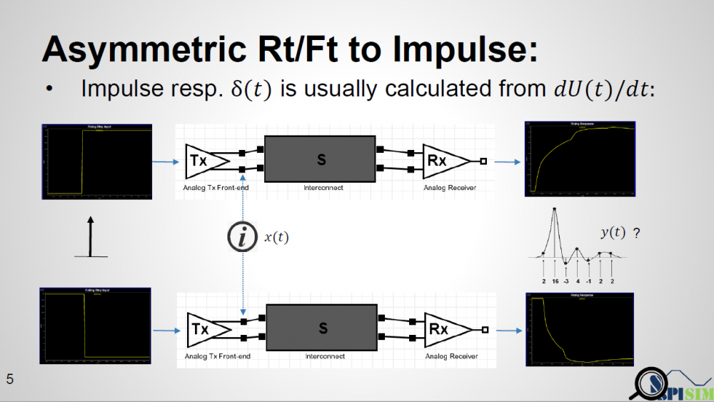
One may think that there is no such limitation that an AMI model can only be called once. So theoretically, a simulator can run analysis flow twice… impulse calculated from rising step response is used for the first time and the one from falling step response is used for the second time. However, not only is this not efficient, a model may not be implemented properly such that calling AMI_Init again right after AMI_Close may cause crash if it’s in the same process and model pointer was not released completely. Thus doing so may hamper a simulator’s robustness.
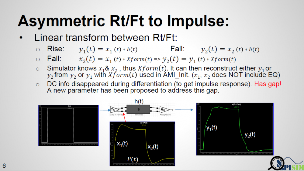
As depicted in the picture above… if a simulator uses a long UI pulse to calibrate the channel, then both rising and falling step response are included in one simulation. Now let the data captured at Tx analog pad as X1 and X2 for rising and falling portion respectively, the data captured at Rx analog pad Y1 and Y2 will be X1 and X2 convolved with interconnect’s transfer function, which is LTI. If we derive a Xform(t) which is transfer function between X1 and X2, then that Xform(t) should also be able to transform between Y1 and Y2. That means if a simulator can calculate Xform(t) it self, then regardless the impulse response it sent to AMI models is calculated from rising or falling step response, it can always “reconstruct” the result from the other type of impulse response using this Xform(t) function.
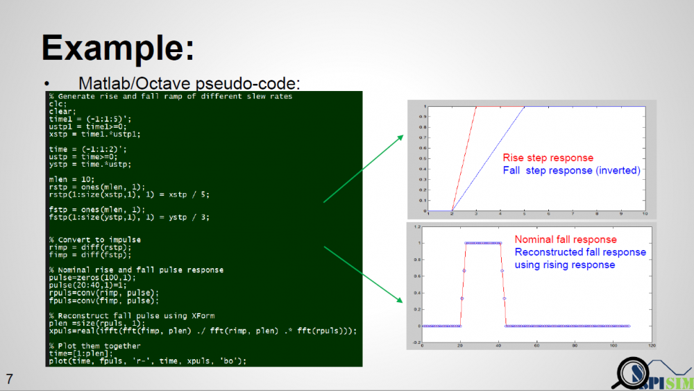
To prove this concept, we have written a simple matlab script taking step inputs of different slew rate, say inp1 and inp2. It calculates the Xform(t) function from both inputs and then reconstruct the response out2′ from out1. When overlaying nominal output out2 and reconstructed out2′ together, we can see that they match very well, thus prove the concept.

Once we have response from both different slew rates, we can construct their respective eyes then use each one’s different portion to construct a synthesized eye. Such eye will not be symmetric like that calculated from SERDES.
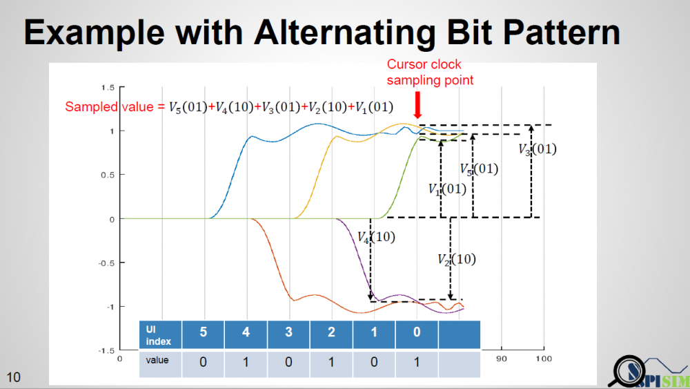
When calculating PDF for asymmetric case, one may also need to consider the precedent bit’s value and use a tree like structure to keep track of possible bit sequence. For example, for a typical SERDES bit sequence, if encoding is not considered, each bit will have 50% one and 50% zero. PDF is constructed based on that assumption. But in an asymmetric case, if the data used at the cursor is from rising response, then the cursor bit must be 1 while (cursor – 1) must be zero. If (cursor – 2) is 1 again, then the tail of falling response at (cursor – 1) will be superimposed to the cursor data. That is, we can’t treat each bit to have same 50% probability when constructing PDF. It’s not a binomial distribution as each occurrence is not independent. A simulator may need to determine the maximum bit length to keep track of first, then based on that depth to form tree-like sequence which leads to the rising or falling steps at the cursor location. Finally use superimpose to construct the overall response.
AMI_GetWave:
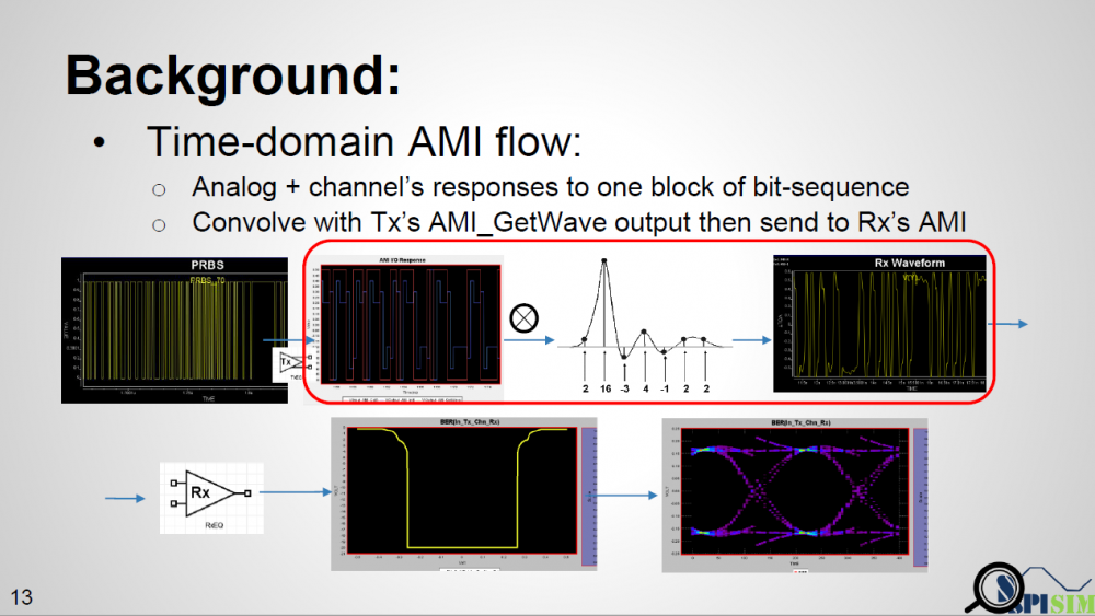
According to the reference flow for the bit-by-bit case: equalized Tx output from digital bit sequence is converted with channel’s impulse response. The resulting waveform is then sent to Rx EQ before getting final results. Either Tx EQ or Rx EQ or both may not be LTI so usage of aforementioned Xform(t) is not applicable.
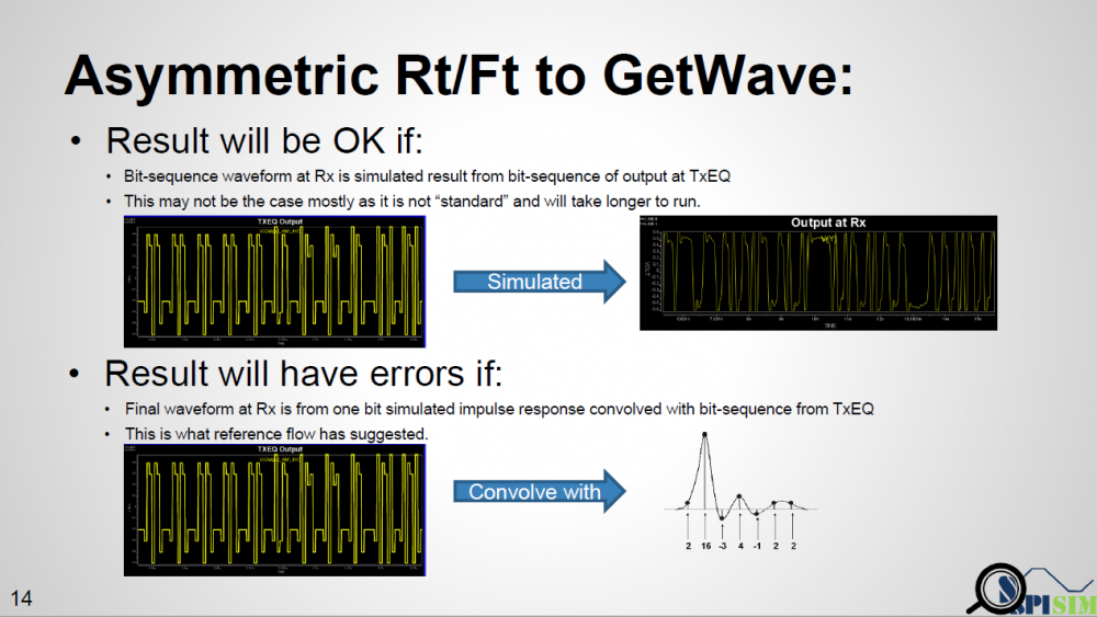
As a fruit of thought… the spec. only mentions that in a bit-by-bit mode, the output of Tx AMI model is equalized digital sequence, while input to the Rx EQ must be the channel response from that sequence, then are there other ways to get such response to Rx yet with different Rt/Ft considered?
One example is like shown in top half of the picture above. If a simulator takes that equalized digital input and “simulate” to get final response, then this “simulation process” should have taken different Rt/Ft into account and has valid results. However, this process will be slow and I don’t think any simulator is doing it this way. Furthermore, the spec. specifically say it needs to “convolve” with impulse response. First of all, this impulse can be from rising or falling. Secondly, even we decide to decovolve with input first (thus has sequences of different delta response) then convolve with pulse response (i.e. one simulated UI), will there be any issue?
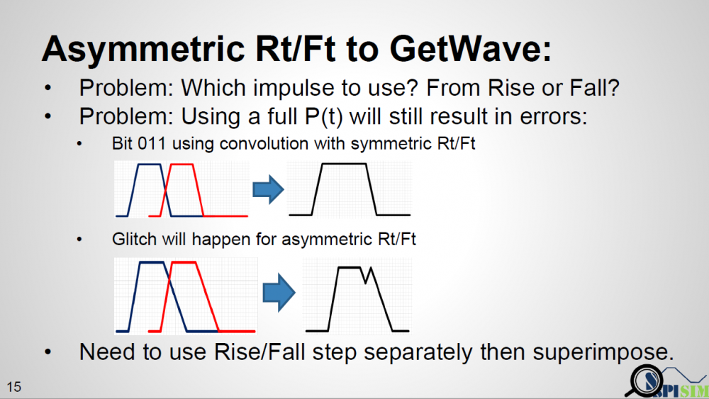
From the plot above… we can see that when a pulse has different rising and falling slew rate, using superimpose to construct 011… will find “glitches” at the trailing high state portion. The severity of this “glitches” depends on how much difference the Rt/Ft is. So using a pulse response here will still not work.
A simple matlab script has also been written to demonstrate occurrence of such “glitches”. This proves that not only using an impulse response to convolve with Tx EQ’s output is problematic, even using a full simulated pulse (which has asymmetric Rt/Ft’s effect) to convolve delta sequences (this delta sequence is original TX EQ’s output deconvolve with one digital bit) will still be problematic. Glitches will happen for consecutive ones or zeros due to the mismatches of Rt and Ft. Thus one must use rise step and fall step response instead when doing such kind of convolution.
Summary:
In this presentation, we discussed how existing AMI flow may be applied to asymmetric Rt/Ft such as those often seen in DDR case. A “smarter” EDA tool should be able to handle this situation without changing on spec.’s reference flow. When a channel analysis is performed in a “statistical” flow, an EDA tool can obtain waveform data at both Tx and Rx analog buffer’s pads during calibration process. Such data can be used to construct a transform function, XForm(t). With this function, impulse response through EQ can be reconstructed and thus built an asymmetric eye. Tree structure may be needed to keep track of possible bit combinations. In a “bit-by-bit” flow, the current spec. may be too specific as it forces to use convolution of TX EQ’s output with channel’s impulse response before sending to RX EQ. Such direct convolution may be problematic. A “smarter” simulator may calculate it using different method without changing data output from TX EQ and input to the RX EQ. Step response should be used as different Rt/Ft will cause “glitches” when consecutive ones/zeros are present if convolution method is used.
Links:
Presentation: [HERE] (http://www.spisim.com/support/paperetc/20180202_DesignConSummit_SPISim.pdf)
Audio recording (English): [HERE]


