S-Param: Various indicators… ILFit, ILD, ICN, ICR, IMR, INEXT, PQM, RQM…

S-Parameter:

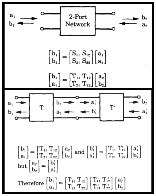
In modern channel design, scattering parameters (S-param) is a commonly used to represent passive interconnects. A S-param model is basically a power view (i.e. incidental and reflective) of each “port” under certain reference impedance at various frequencies. So its format is like a frequency dependent matrices each with dimensions equivalent to the square number of ports. In a college text-book, a two port network is usually used to explain these incidental/reflective relationships. Using linear algebra, different form (Z, Y, T, ABCD etc) may also be calculated to be used in different scenarios. One can also cascade two or more S-param. together to form a consolidated S-param model.

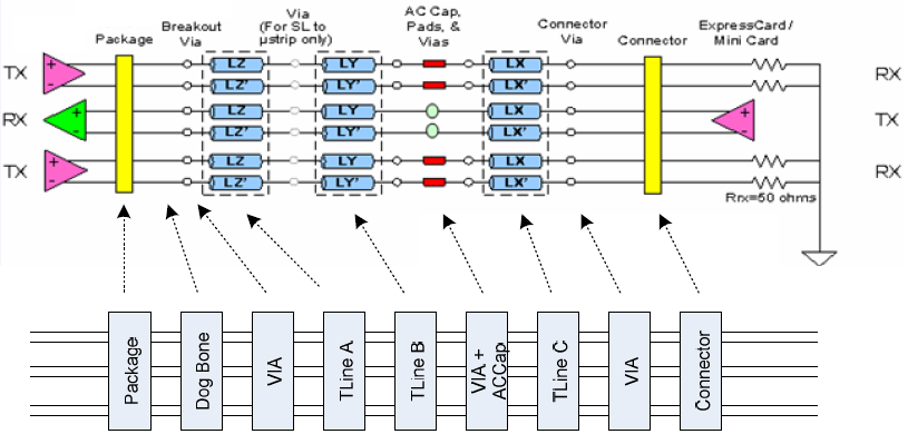
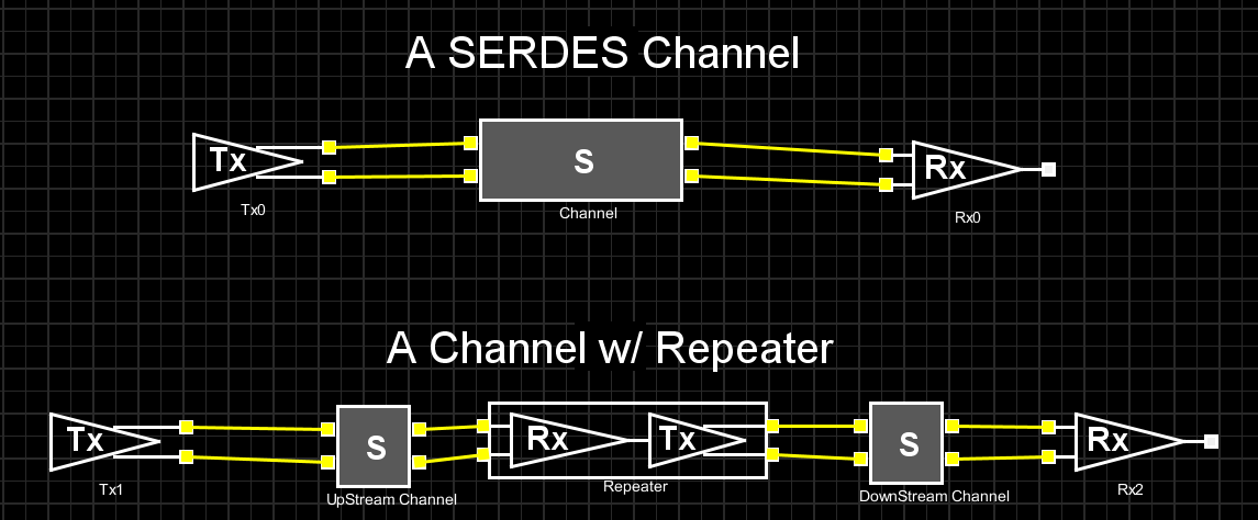
For example, a typical SERDES channel is usually in point-to-point topology. So stages of various interconnects may be cascaded into a single S-parameter.

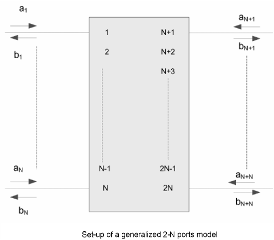
Usually an 3D field solver tool like HFSS/Q3D etc will extract physical design into a S-parameter.  For a homogeneous interconnect such as transmission line, 2D/2.5D field solver can be used to extract their RLGC/tabular model data. These RLGC data can easily be converted to corresponding S-parameters. So essentially all these stages’ device model can be in S-param. format and cascaded together. However, when there are more than two ports on each side… such as the schematic shown above, the basic two-port network formulas need to be “generalized” so that plain S/Z/Y/T/ABCD conversion formula can still be applied. That is, the ports needs to be arranged in such a way so that a “generalized 2-N ports” can be formed:

As a S-parameter is passive in nature and represent “power” data, its value or “decay” can be viewed in dB scale and considered as a type of “loss” (compare to 0Hz origin, or 0dB). Depending on the incidental (through-type) or reflective relationship between each ports, different part of S-param may be viewed as “insertion loss (IL)” or “return loss (RL)” from near end (NE) or far-end (FE):

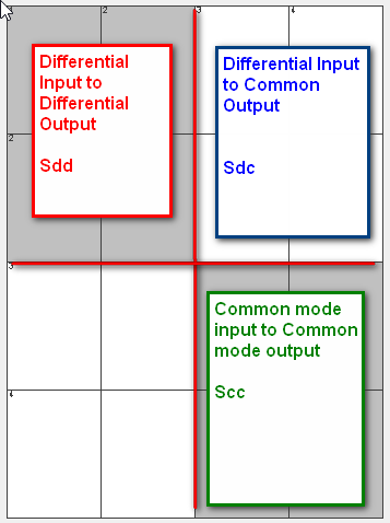
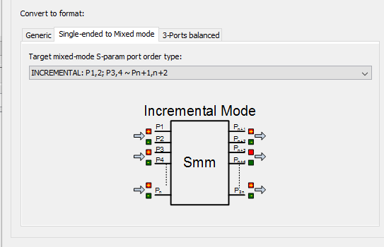
The notation above is for a “single-ended” s-param. To describe a differential channel, a “differential-mode” or “mixed-mode” conversion need to be applied. The forming  of “differential” relationship is essentially to subtract certain element in the S-param’s matrix which represents the “return” path or return channel. The resulting S-parameter can thus be used to describe relationship between “modes” such as differential mode or common mode:

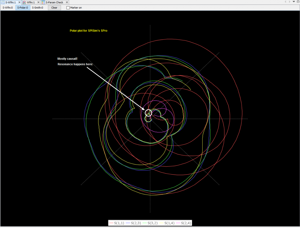
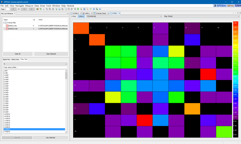
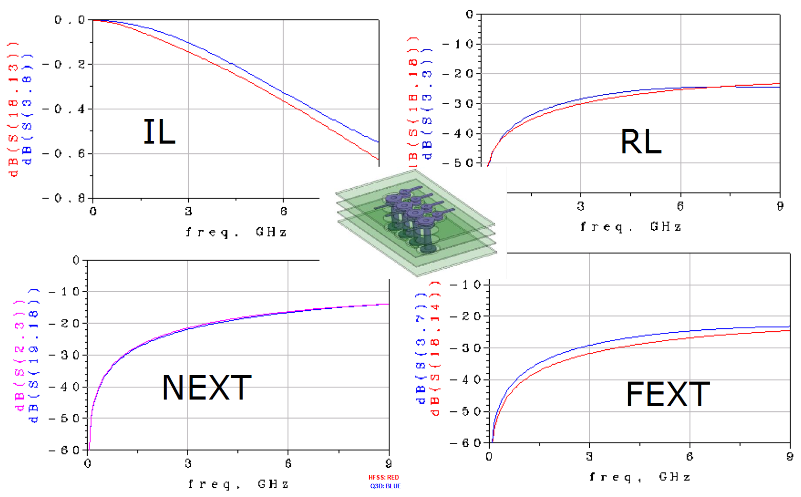
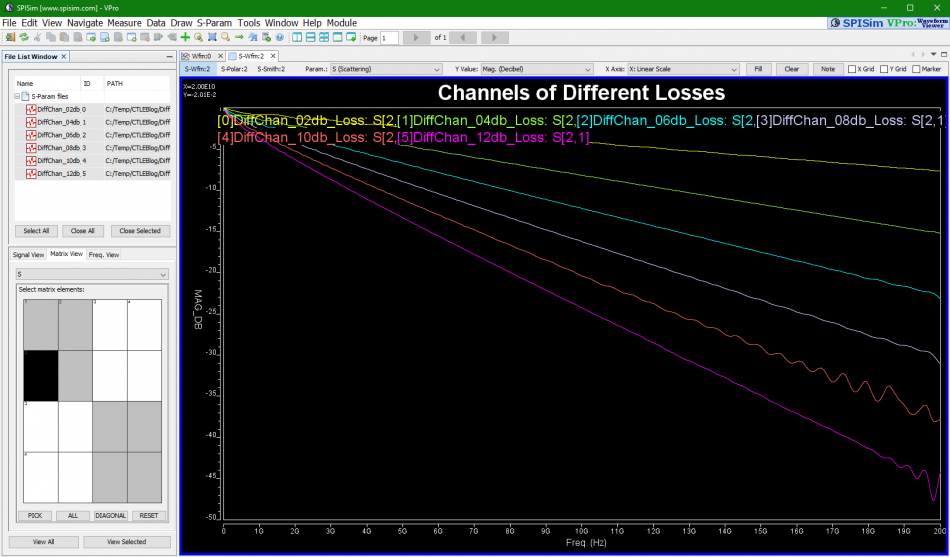
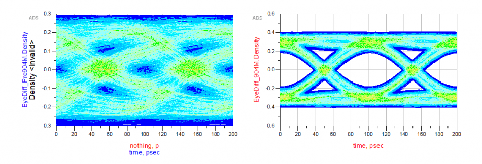
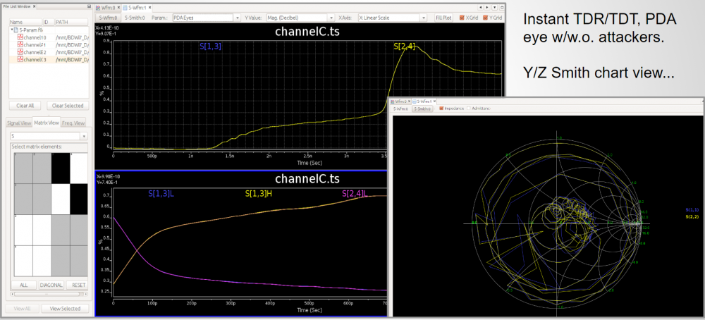
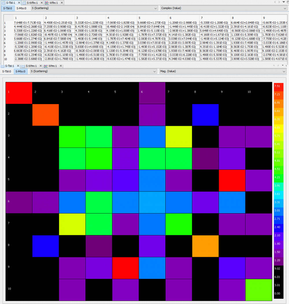
As one can see, a s-parameter is so “versatile” in describing interconnect’s properties yet its data is non-intuitive complex numerical matrices, an usual or traditional way of checking a s-param’s quality is to visualize its data and “eye-balling” to correlate to model data from previous design revision or results from different extractors:

While this method is still useful, the judgement of model’s quality very much depends on one’s experience or tolerance and thus is not very objective. As the data rate becomes higher and interconnect becomes more “coupled” or lossy, new parameters are defined to check a S-parameter’s figure of merits.

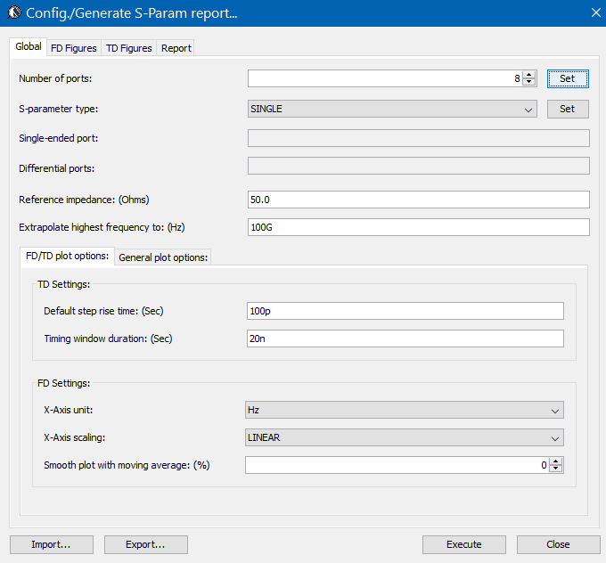
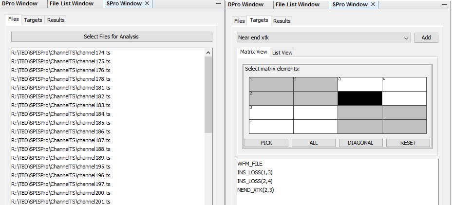
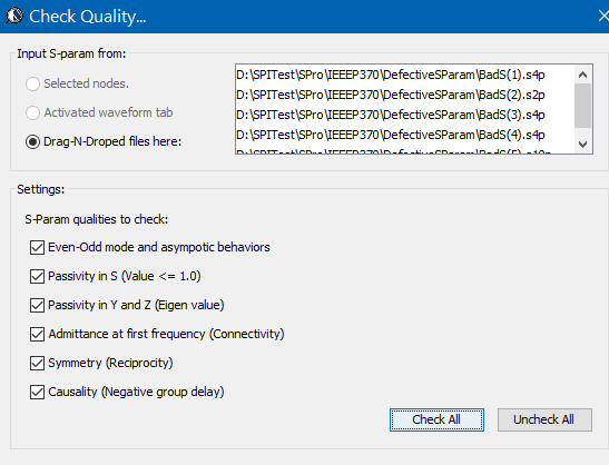
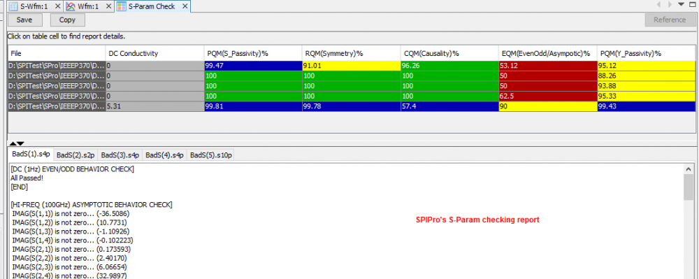
Here we list some of important and non interface specific S-parameter checking parameters for reader’s reference. Many of these quality metrics have been incorporated into our SPISPro module for an one stop shop of all the S-param. processing needs.

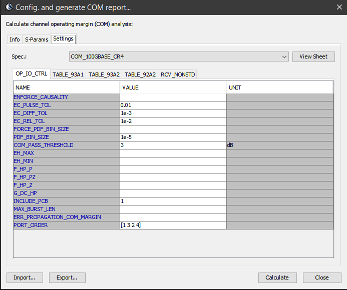
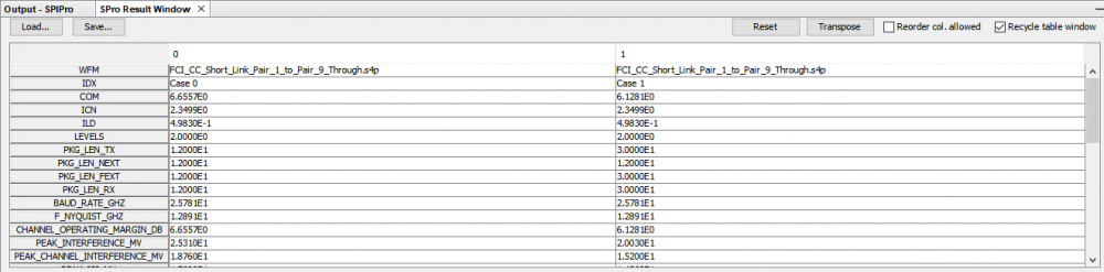
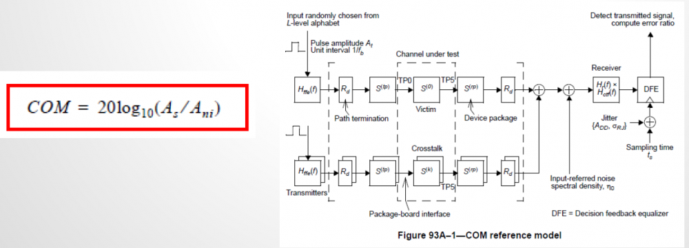
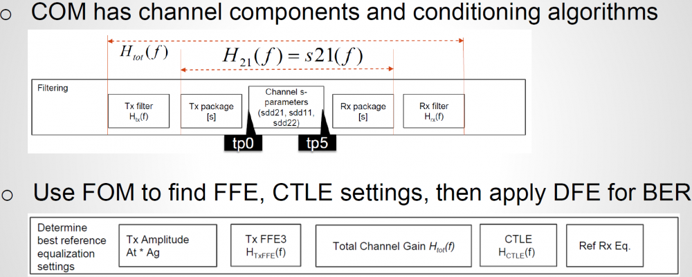
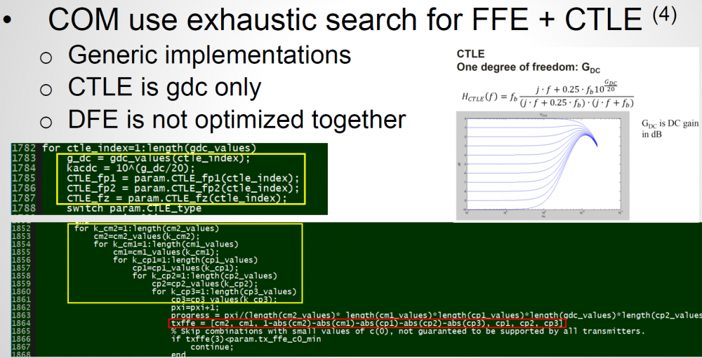
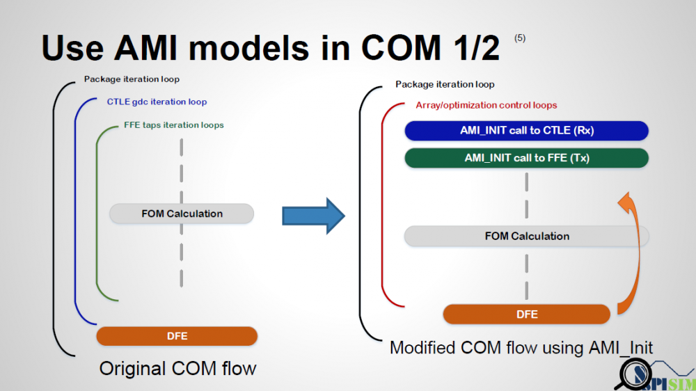
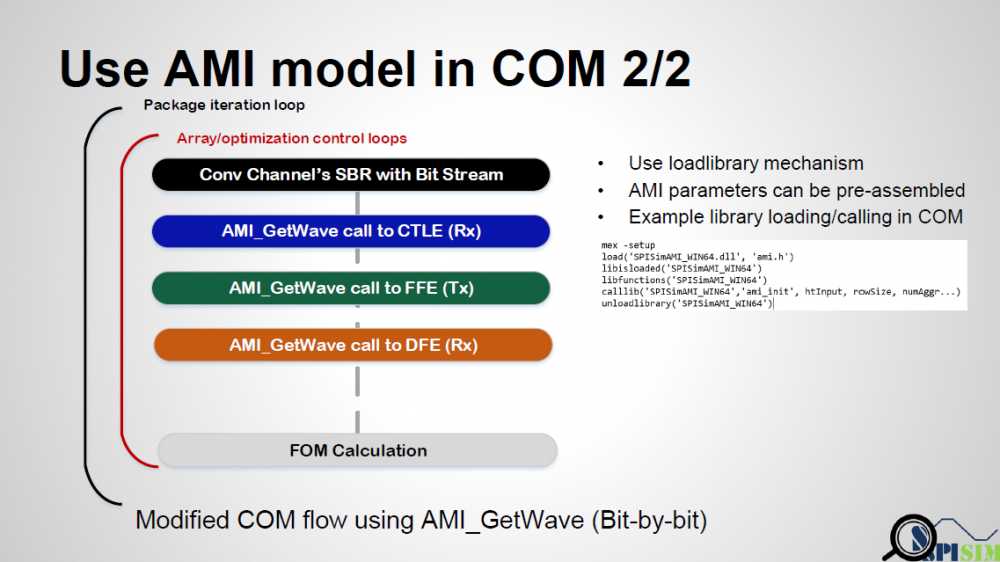
S-param. check introduced in IEEE 802.3 bj: This spec. defines a “figure of merit” for each interconnect used in a high-speed SERDES (>= 100G) channel. Generic package and motherboard portion are included using behavior models and cascaded with user provided through-type/NEXT/FEXT S-parameter to form a complete and consolidated channel. Then parameters of FFE at the Tx and CTLE+DFE at the Rx are swept to see how good a channel can perform in the best scenarios . A calculated “COM” (channel operating margin” value is then calculated to represent this channel’s potential. COM’s value is significantly affected by cascaded S-param’s parameters listed below:

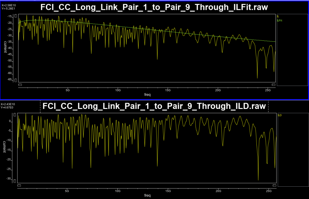
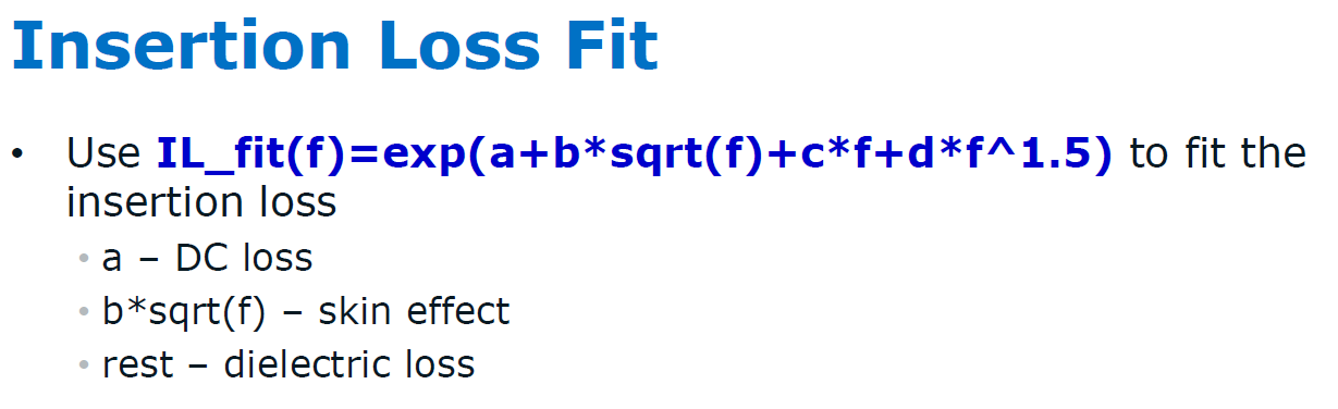
  • ILFit: Insertion loss fit

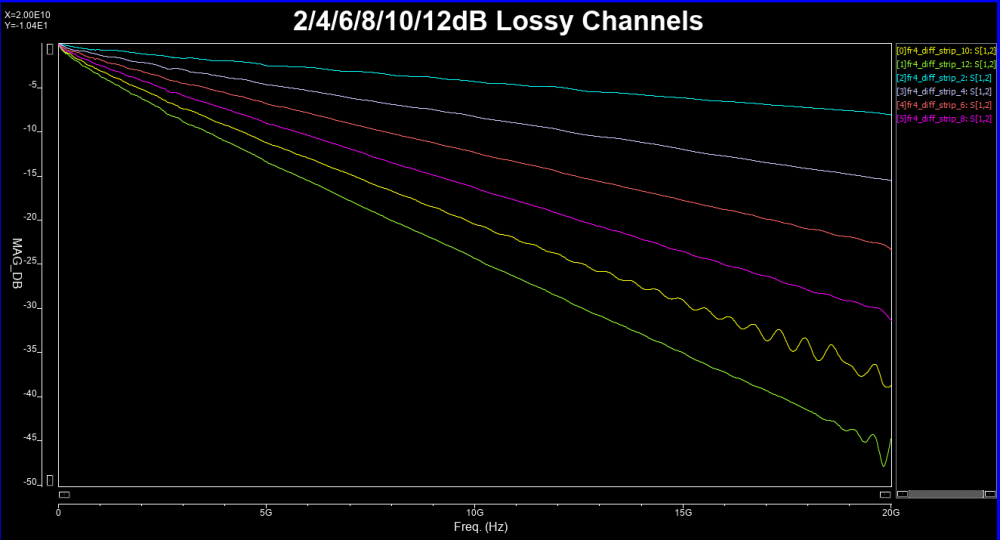
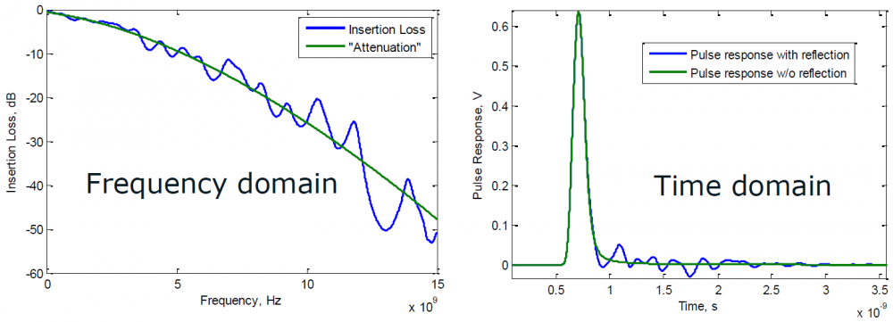
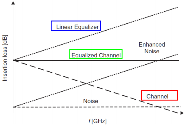
The inductive and capacitive properties of a channel will introduce frequency dependent loss. To avoid signal distortion, it is usually desired to have a linear relationship between frequency and the channel losses such as well-behaved example below:

However, due to impedance mismatch and multiple reflections, such linear dependency may not be possible. Thus “ripples” may exist which in terms introduce the time domain noise and causes degraded final eye height/width. A “fitted-curve” (ILFit, up to half of bandwidth, i.e. Nyquist rate) may be introduced to approximate such insertion loss. Such smoothed curve can be viewed as channel without mutli-reflection and is thus a “best-case” scenario.

ILfit is usually calculated in a minimized-squared-error (MSE) sense. Pre-defined curve’s order is used and its weighted parameters are then fitted.

  • ILD: Insertion loss deviation

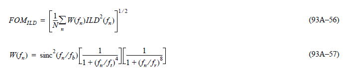
Once an ILfit is calculated, one can calculate the “difference” between Ithis fitted curve and original data to form the ILD:

The calculated ILD values can then be further integrated to form a channel’s Figure of merits”:

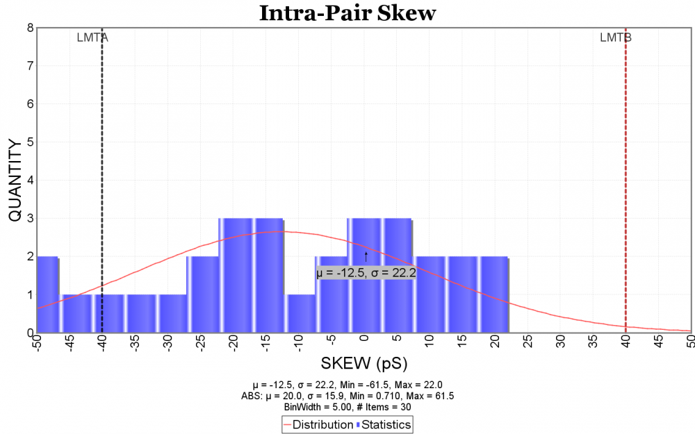
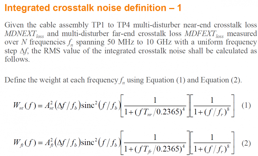
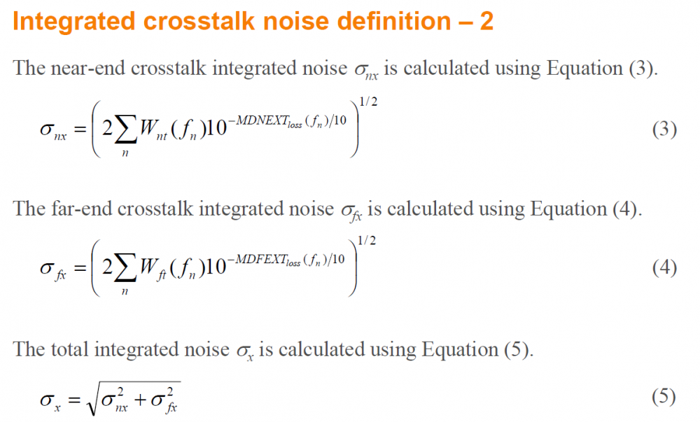
  • ICN/ICF: Integrated NE/FE cross-talk noise

These are calculated RMS values integrated (summed) over a frequency range. The integrated value represents impact due to both near-end and far-end crosstalk:

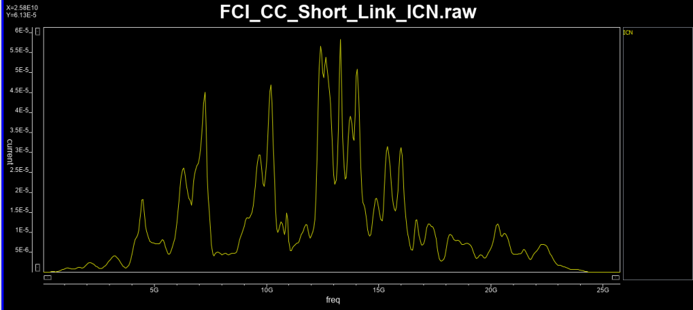
  • ICR: Insertion loss to cross-talk ratio

This value compares channel performance’s impact due to insertion loss vs cross-talk.

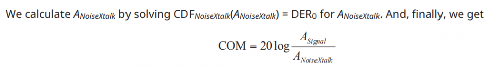
  • COM: Channel operating margin

The amplitude resulting from single-bit-response (SBR) can be separated based on the signal and losses due to crosstalk, insertion loss etc. With equalization at both Tx and Rx side both being taken into account, the best case value will eventually be summarized as an indicator, “COM” for the channel performance’s comparison.

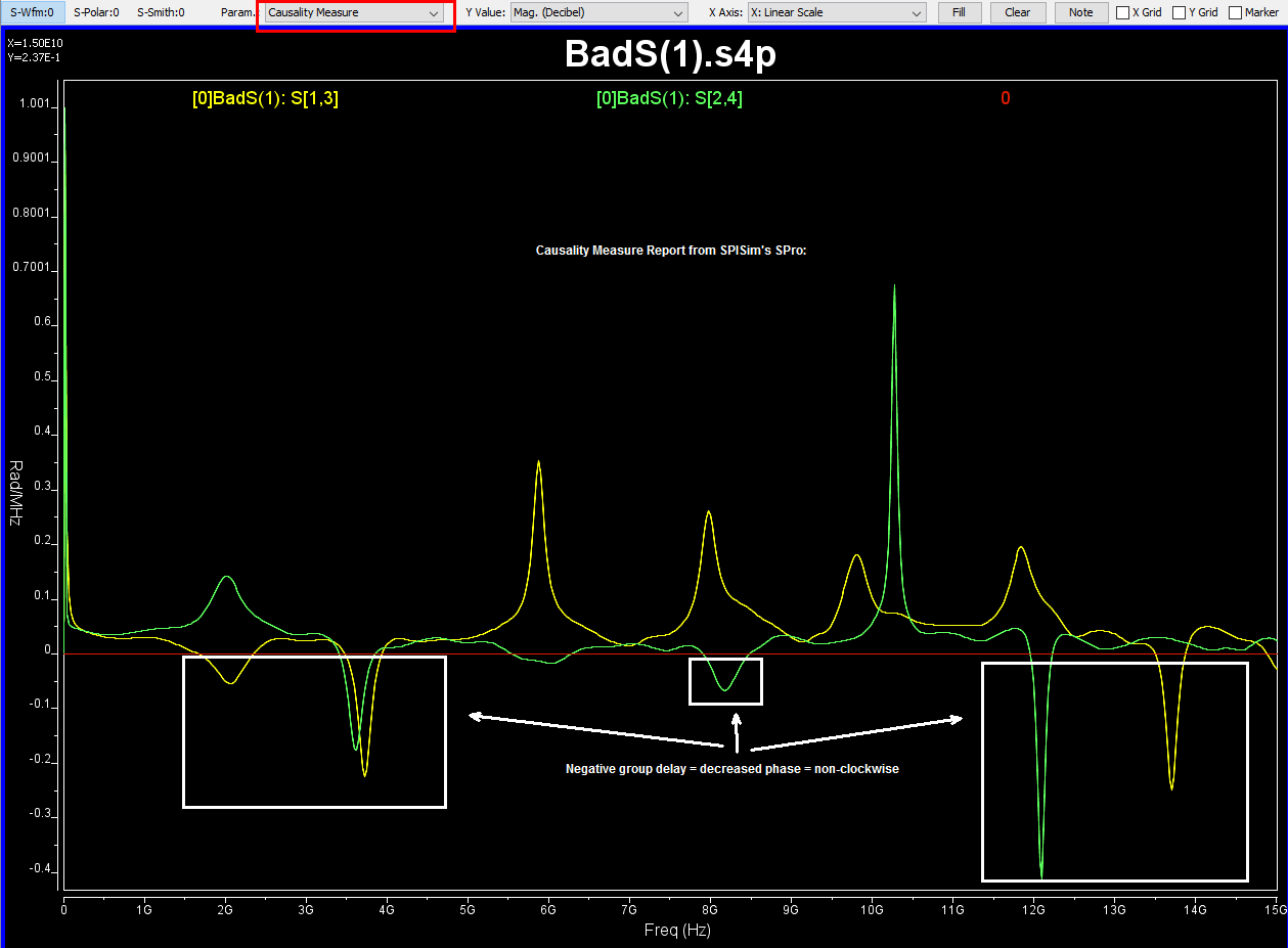
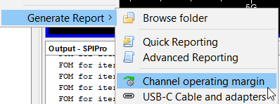
S-param check and parameters defined in COM methodologies has profound impact. It not only sets an example for other interfaces (e.g. USB-C, discussed below) to check their interconnect model, but also provides a meaningful correlation between different S-param’s deviation toward its final eye impact. Details about these calculation can be found in 802.3bj spec.. SPISim’s SPro integrated COM as part of the S-param reporting flow as shown in various plots above and screen shots below:


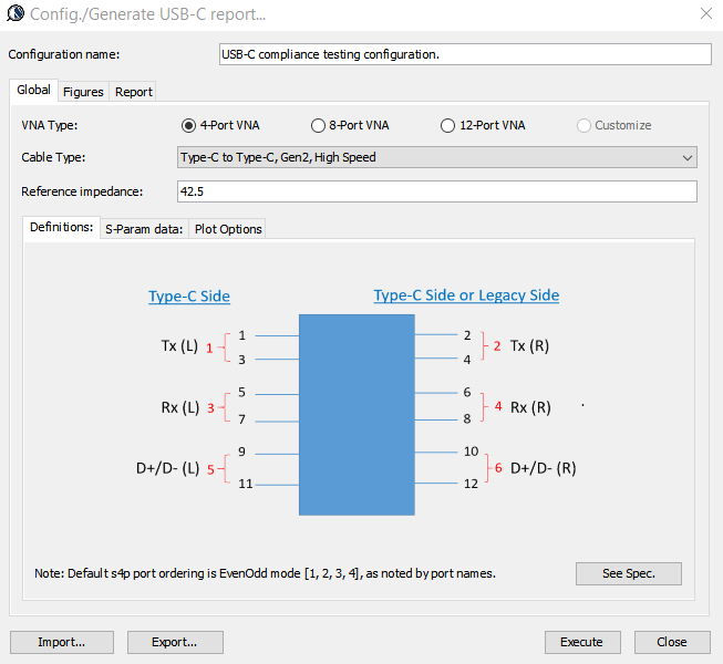
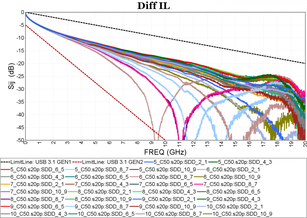
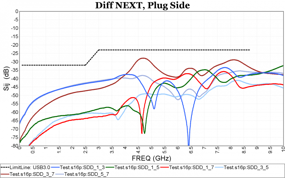
S-param. check introduced in USB-C Cable/Connector:

USB Type C (USB 3.1) spec. was published in 2014. Not only does it increase the signaling speed from previous gen. to be 10Gbps, it also provides power charging capability, has a smaller connector form factor and has non-directional connectivity. As this spec. is back-ward compatible, both legacy and low-speed USB connectivity are also supported. As such, there are many different scenarios, coupled with different VNA capabilities to be considered:

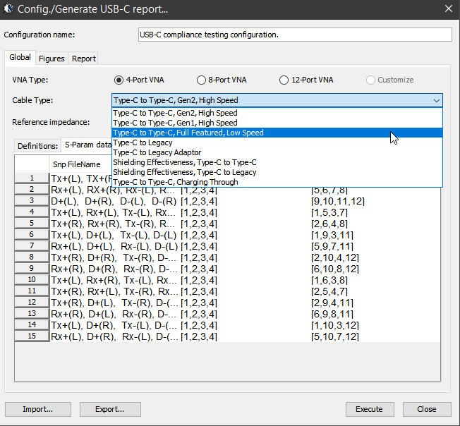
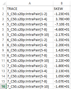
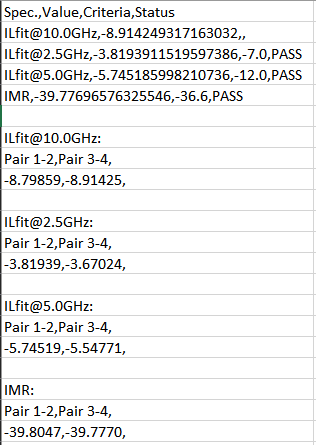
However, the main check (ILD/IMR etc) in USB-C is more or less similar to those used in COM methodology. Nevertheless, there are still minor difference in terms of implementation such as how insertion loss should be fitted and weighted…. as discussed below. In addition, since there are different pairs of traces (e.g. SS, D+/D- etc) in the cable/connector, dedicated checks between signals are also included. Essentially they are calculation applied toward specific S-parameter matrix elements corresponding to the incidental/reflective behaviors between those traces/ports.

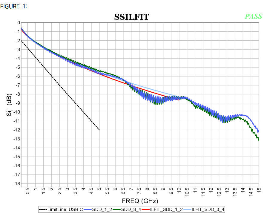
  • ILfitNq: Insertion loss fit at Nyquist rate

COM methodology in 802.3bj spec. spells out what the fitting formula should be used. However, this is not the case for USB-C. In a reference materials for the USB-C dev. forum’s tool, Interpar, it suggests a different formula as shown below should be used:

In addition, a “weighting” function is suggested to downplay the deviation at the high-frequency portion:

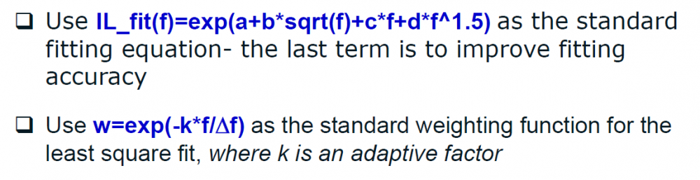
The checking of the IL_Fit/ILD relies more on frequency dependent spec. lines as well up to the Nyquist rate. A “Pass”/”Fail” indicator is then calculated against these spec. line.

  • IMR: Integrated multi-reflection

The deviation part (ILD) has been separated to form its own figure of merit using formula shown below:

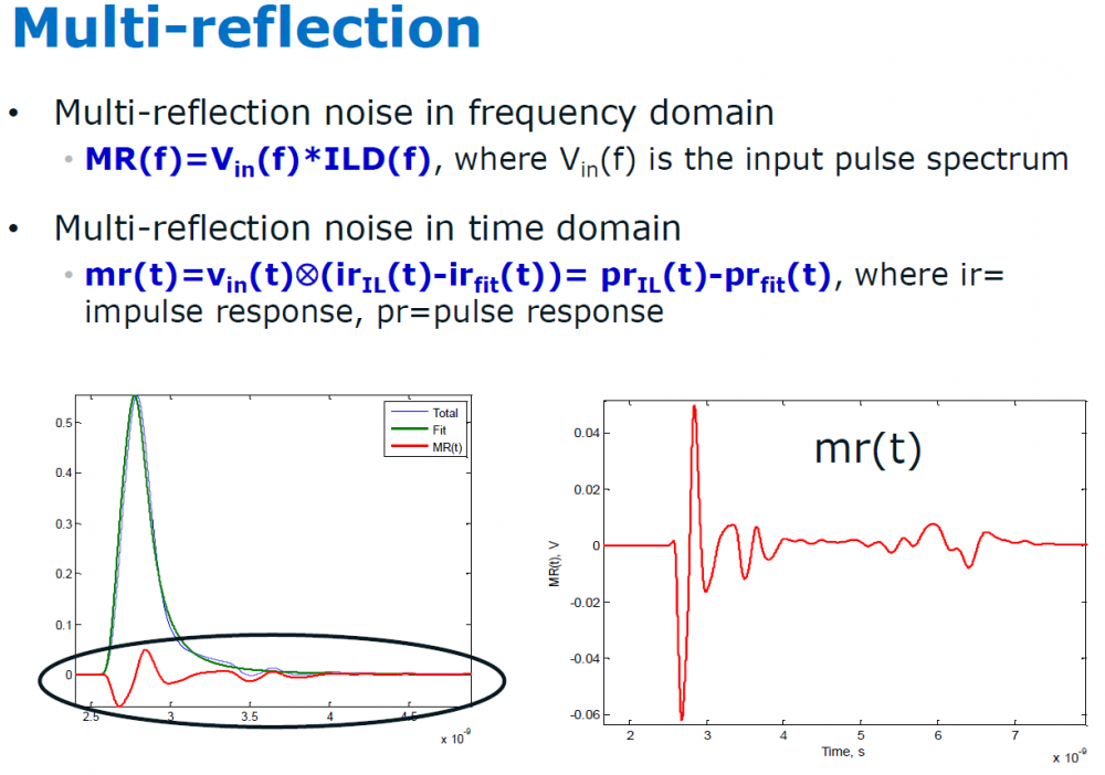
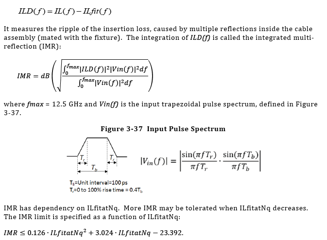
Resulting IMR values are super-speed pair (SS) specific:

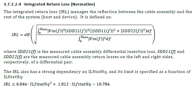
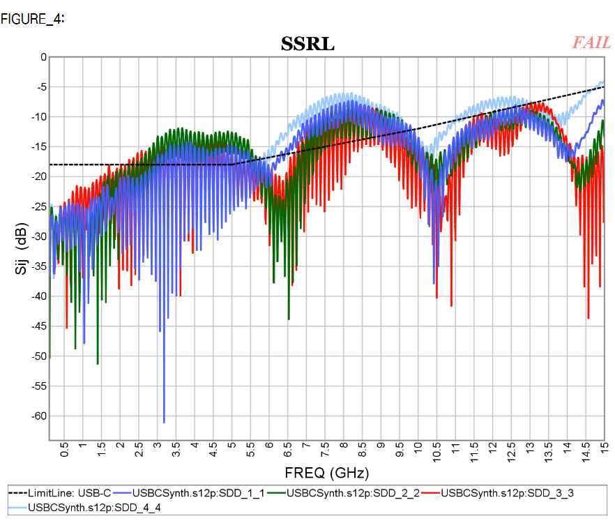
  • IRL: Integrated return loss

This is a metric dedicated for return loss check:

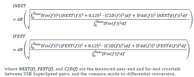
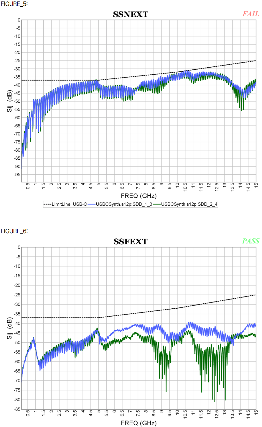
  • INEXT/IFEXT: Integrated NEXT/FEXT noise

Similarly, there are metric dedicated for cross talk check and spec-lines:

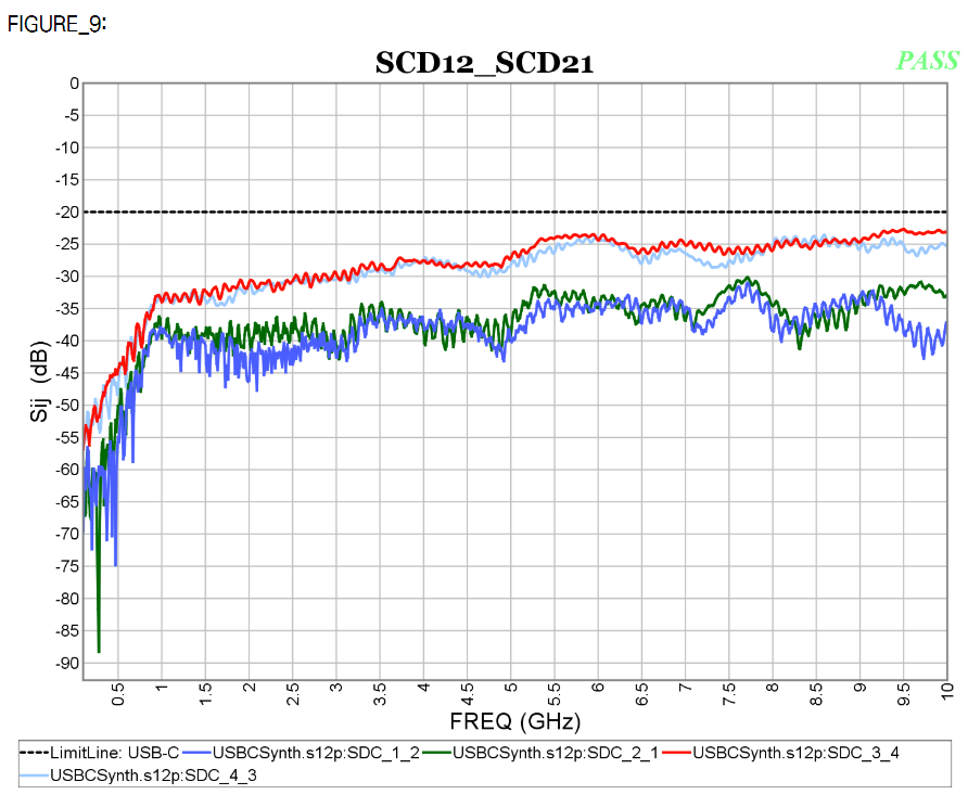
  • Others: other signal specific check can be performed by simply configuring and plotting specific matrix elements within certain frequencies ranges then compare with defined spec. lines. Example of differential-to-common mode conversion is shown below.

  Both COM and USB-C S-param methodologies are parts of our SPro’s reporting flow:

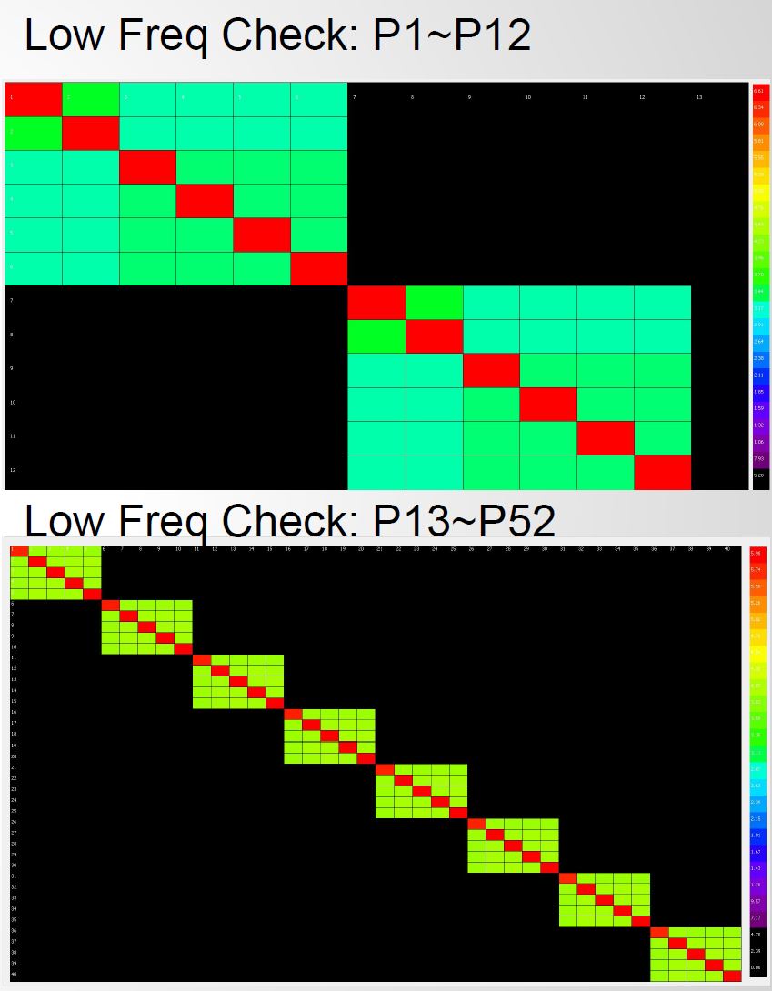
S-param check introduced in IEEE P370:

IEEE P370 committee’s objective is to define fixture design as well as data quality metric standard for high speed interconnects. A good overview article is available at the signal integrity journal linked [HERE] The P370 WG3, which us SPISim took part in, focuses on S-parameter’s various quality metric (QM):

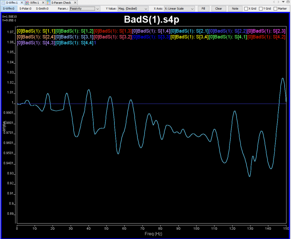
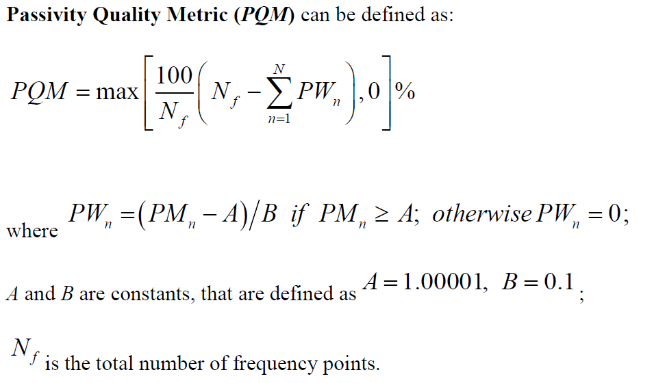
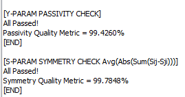
  • PQM: S/Y-Passivity quality metric
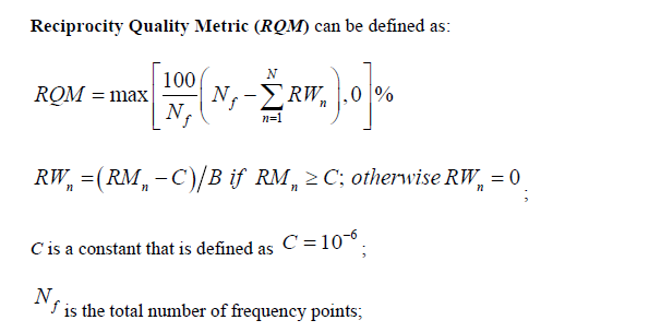
  • RQM: Reciprocal/symmetry quality metric
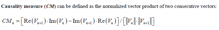
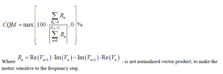
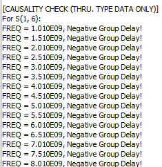
  • CQM: Causality quality metric
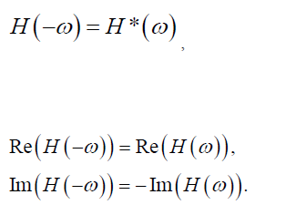
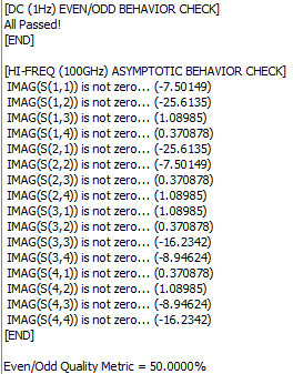
  • EQM: Even-Odd quality metric

Previously, we have written a post [LINKED HERE] detailing how these metrics are calculated. Interested readers may also wait for upcoming P370 spec. for the details. One thing to note is that regardless it’s COM, USB-C or channel simulation like those involved IBIS-AMI models, high-quality interconnect/S-param model is usually required as it will significantly impact the resulting impulse response or pulse/single-bit response. When convolving these time-domain responses many times to obtain final PDF/CDR for BER, any initial imperfection in the S-param model will be “amplified” and cause end results’ error. As such, in both COM and USB-C’s flow, the cascaded or user measured S-param have always been checked and adjusted particularly in the aspects of passivity and causality. They are done particularly at the low (toward DC) and high frequency (trailing tails) region. Separated procedures have been applied to extrapolate for a DC point by using first several data points then fit with “theoretical” good behavior model equation to make sure DC response is correct. These details are not even mentioned in the 802.3/USB-C spec…. one must bite the bullet and study to their reference implementation (e.g. matlab scripts) to find such procedure’s existence. Without this auto fixing, calculated COM/Spec. parameters will not match those produced by reference script or InterPar forum tool.

IBIS-AMI: Something about CTLE

Overview:

Continuous time linear equalizer, or CTLE for short, is a commonly used in modern communication channel. In a system where lossy channels are present, a CTLE can often recover signal quality for receiver or down stream continuous signaling. There have been many articles online discussing how a CTLE works theoretically. More thorough technical details are certainly also available in college/graduate level communication/IC design text book. In this blog post, I would like to focus more on its IBIS-AMI modeling aspect from a practical point of view. While not all secret sauce will be revealed here:-), hopefully the points mentioned here will give reader a good staring point in implementing or determining their CTLE/AMI modeling methodologies.

[Credit:] Some of the pictures used in this post are from Professor Sam Palermo’s course webpage linked below. He was also my colleague at Intel previously. (not knowing each other though..)

ECEN 720: High-Speed Links Circuits and Systems


What and why CTLE:

The picture above shows two common SERDES channel setups. While the one at the top has a direct connection between Tx and Rx, the bottom one has a “repeater” to cascade up stream and down stream channels together. This “cascading” can be repeated more than once so there maybe more than two channels involved. CTLE may sit inside the Rx of both set-ups or the middle “ReDriver” in the bottom one. In either case, the S-parameter block represents a generalized channel. It may contain passive elements such as package, transmission lines, vias or connectors etc. A characteristic of such channel is that it presents different losses across spectrum, i.e. dispersion.

For example, if we plot these channel’s differential input to differential output, we may see their frequency domain (FD) loss as shown above.

Digital signals being transmitted are more or less like sequence of bit/square pulse. We know that very rich frequency components are generated during its sharp rising/falling transition edges. Ideally, a communication channel to propagate these signals should behave like an (unit-gain) all pass filter. That is, various frequency components of the signal should not be treated equally, otherwise distortion will occur. Such ideal response can be indicated as the green box below:

In reality, such all pass filter does come often. In order to compensate our lossy channels (as indicated by the red box) to be more like the ideal case (green box) as an end result, we need to apply equalization (indicated by blue box). This is why an equalizer is often used… basically it provides a transfer function/frequency response to compensate the lossy channel in order to recover the signal quality. A point worth taken here is that the blue box and red box are “tie” together. So using same equalizer for channels of different losses may cause under or over compensated. That is, an equalizer is related to the channel being compensated. Another point is that CTLE is just a subset of such linear equalizer.

CTLE is a subset of linear equalizer:

A linear equalizer can be implemented in many different ways. For example, a feed-forward equalizer is often used in the Tx side and within DFE:

FFE’s behavior is more or less easier to predict and its AMI implementation is also quite straight forward. For example, a single pre-tap or post-tap’s FFE response can be easily visualized and predicted:

Now, a CTLE is a more “generalized” linear equalizer, so its behavior is usually represented in terms of frequency responses. Thus, to accommodate/compensate channels of different losses, we will have different FD responses for CTLE:

Now that IBIS-AMI modeling for CTLE is of concern, how do we obtain such modeling data for CTLE and how they should be modeled?

Different types of CTLE modeling data:

While CTLE’s behavior can be easily understood in frequency domain, for IBIS-AMI or channel analysis, it eventually needs to come back to time domain (FD) to convolve with inputs. This is because both statistical or bit-by-bit mode of link analysis are in time domain. Thus we have several choice: provide model FD data and have it converted to TD inside the implemented AMI model, or simply provide TD response directly to the model. The benefit of the first approach is that model can perform iFFT based on analysis’ bit rate and sampling rate’s settings. The advantage of the latter one is that the provided TD model can be checked to have good quality and model does not need to do similar iFFT every time simulation starts. Of course, the best implementation, i.e. like us SPISim’s approach, is to support both modes for best flexibility and expandability 🙂

  • Frequency domain data:

Depending on the availability of original EQ design, there are several possibilities for FD data: Synthesized with poles and zeros, extract from S-parameters or AC simulation to extract response.

  1. Poles and Zeros: Given different number of poles, zeros and their locations along with dc boost level, one can synthesize FD response curves:
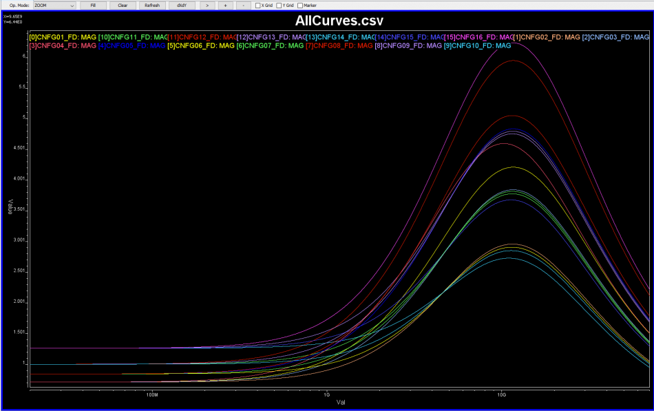
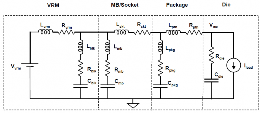
So say if we are given a data sheet which has EQ level of some key frequencies like below: Then one can sweep different number and locations of poles and zeros to obtain matching curves to meet the spec.:
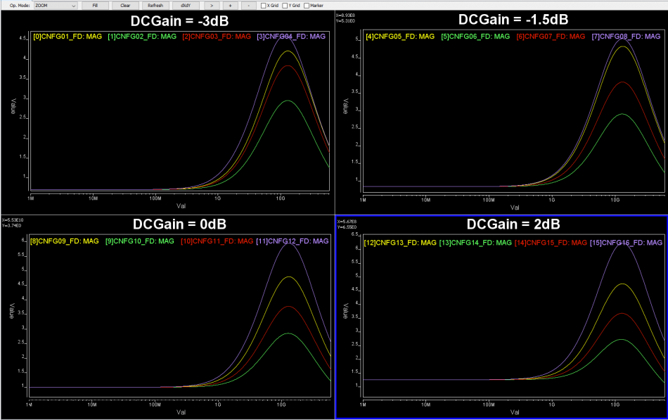
Such synthesized curves are well behaved in terms of passivity and causality etc,  and can be extended to covered desired frequency bandwidth.
  2. Extract from S-parameters: Another way to obtain frequency response is from EQ circuit’s existing S-parameter. This will provide best correlation scenarios for generated AMI model because the raw data can serve as a design target. However, there are many intermediate steps one have to perform first. For example, the given s-parameter may be single ended and only with limited frequency range (due to limitation of VNA being used), so if tool like our SPISim’s SPro is used, then one needs to: reording port (from Even-Odd ordering, i.e. 1-3, 2-4 etc to Sequential ordering, i.e. 1, 2 -> 3, 4), then convert to differential/mixed mode, after that extrapolate toward dc and high frequencies (many algorithms can be used and such extrapolation must also abide by physics) and finally extract the only related differential input -> differential output portion data.
  3. AC simulation: This assumes original design is available for AC simulation. Such raw data still needs to be sanity checked in terms of loss and phase change. For example, if gain are not flat toward DC and high-frequency range, then extra fixing may be needed otherwise iFFT results will be spurious.
  • Time domain data: time domain response can be obtained from aforementioned FD data by doing iFFT directly as shown below. It may also be obtained by simulating original EQ circuit in time domain. However, there are still several considerations:
  1. How to do iFFT: padding with zeros or conjugate are usually needed for real data iFFT. If the original FD data is not “clean” in terms of causality, passivity or asymptotic behavior, then they need to be fixed first.
  2. TD simulation: Is simulating impulse response possible? If not, maybe a step response should be performed instead. Then what is the time step or ramp speed to excite input stimuli? Note that during IBIS-AMI’s link analysis, the time step being used there may be different from the one being used here, so how will you scale the data accordingly. Once a step response is available, successive differentiation will produce impulse response with proper scaling.

How to implement CTLE AMI model:

Now that we have data to model, how will they be implemented in C/C++ codes to support AMI API for link analysis is another level of consideration.

  • Decision mechanism: As mentioned previously, a CTLE FD response targets at a channel of certain loss, thus the decision to use appropriate CTLE settings based on that particular channel at hand must either be decided by user or the model itself. While the former (user decision) does not need further explanation, the latter case (model decision, i.e. being adaptive) is a whole different topic and often vendor specific.

Typically, such adaptive mechanism has a pre-sorted CTLE in terms of strength or EQ level, then a figure-of-merit (FOM) needs to be extracted from equalized signal. That is, apply a tentative CTLE to the received data, then calculate such FOM. Then increase or decrease the EQ level by using adjacent CTLE curves and see whether FOM improves. Continue doing so until either selected CTLE “ID” settles or reach the range bounds. This process may be performed across many different cycles until it “stabilized” or being “locked”. Thus, the model may need to go through training period first to determine best CTLE being used during subsequent link analysis.

  • EQ configurations:

So now you have a bunch of settings or data like below, how should you architecture the model properly such that it can be extended in the future with revised CTLE response or allow user to perform corner selections (which essentially adds another dimension):

This is now more in software architecture domain and needs some trade-off considerations. For example, you may want to provide fine grid full spectrum FD/TD response but the data will may become to big. So internal re-sampling may be needed. For FD data, the model may needs to sample to have 2^N points for efficient iFFT. Different corner/parameter selection should not be hard coded in the models because future revised model’s parameter may be different. For external source data, encryption is usually needed to protect the modeling IP. With proper planning, one may reuse same CLTE module in many different design without customization on a case-by-case basis.

  • Correlations:

Finally it’s time to correlate the create CTLE AMI model against original EQ design or its behavioral model. Done properly, you should see signals being “recovered” from left to right below:

However, getting results like this in the first try may be a wishful thinking. In particular, the IBIS-AMI model does not work alone… it needs to work together with associated IBIS model (analog front-end) in most link simulator. So that IBIS model’s parasitics and loading etc will all affect the result. Besides, the high-impedance assumption of the AMI model also means proper termination matching is needed before one can drop them in for direct replacement of existing EQ circuit or behavioral models for correlation.

Summary:

At this point, you may realize that while a CTLE can be easily understood from its theoretic behavior perspective, its implementation to meet IBIS-AMI demands is a different story. We have seen CTLE models made by other vendor not expandable at all such that the client need to scratch the existing ones for minor revised CTLE behavior/settings (also because this particular model maker charges too much, of course). It’s our hope that the learning experience mentioned in this post will provide some guidance or considerations regardless when you decide to deep dive developing your own CTLE IBIS-AMI model, or maybe just delegate such tasks to professional model makers like us 🙂

IBIS-AMI: Using IBIS-AMI in COM Analysis

[This blog post is written in preparation for the presentation of the same title to be given at the 2018 DesignCon IBIS Summit. Presentation slides and audio recording are linked at the bottom of this post.]

Motivation:

An AMI model is in the binary form of .dll (dynamic link library) or .so (shared object). It itself is not an executable and can’t be used directly. To load or run the AMI models, one needs to have a “driver”. Commercial tools like HSpice has a license required utility called “AMICheck” to test drive the given AMI models with rise/fall/single bit response. We SPISim also provide a free utility called SPISimAMI.exe which does pretty much the same. These small drivers are good when you want to quickly check whether the AMI models at hand are “run-able”. However, to validate or test model’s full function, such a simple tester is often insufficient. In an ideal situation, a link analysis simulator, which will load Tx and Rx AMI models involved and perform calculation/optimization, is preferred as a driver. If a model developer can use IDE to attach to this simulator process and have access to the simulator codes as well, then he/she can set a break point within both simulator and the loaded AMI model to step through and debug during the whole analysis process.

Even if one doesn’t have access to simulator’s codes or debug build, theoretically, an IDE can also “attach” to a process before it loads the AMI dlls in which we have break points set (as a model builder, we have access to the model codes). However, thing is not so straight forward in real world. Most of the EDA tools I have seen allow user to interact different link analysis settings via GUI, then when a “simulate” button is clicked, a separated process is launched/forked and that process will do the work such as characterizing channel, loading AMI models and simulation etc before giving results back to the front-end GUI for further display. It is not easy (if even possible) to automatically attach dll files being debugged to these “spawn/forked” process. No to mention that if both Tx and Rx models are involved in a optimization process (such as back-channel), then simply stopping at a breaking point within one of the AMI models is not enough… one can’t observe and see the interactions for full picture. With these limitations, develop and testing AMI models within a full link analysis flow become challenging.

For a model developer who does not have access to these full link simulator’s sources, open source platform is a direction. There are several ones out there already… PyBert and COM are two such examples. From what I have seen, most of them already have some generic Tx/Rx algorithm blocks in place. So these EQ operating portions may be replaced to support AMI models to meet our needs. Being able to do so will shorten the model design cycle and enable the possibility to develop blocks with more advanced capabilities (such as back-channel communication). As PyBert already has some sort of AMI modeling support, this paper intends to explore possibilities to add similar capabilities in IEEE 802.3 spec. supported channel operating margin (COM) flow.

Background:

Channel Operating Margin (COM) is a ratified IEEE802.3 spec. Interested reader can find an overview slides given by the COM main author (also my former colleague at Intel) linked here: [Channel Operating Margin Tutorial] More detailed technical details are available in the IEEE 802.3BJ spec document and Richard’s 2013 DesignCon paper of same title. Further more, its matlab source codes are also available at the 802.3 website.

Given such technical depth like COM’s, to describe it in several paragraphs in this post will not be meaningful. So I will try to just give an overview from AMI builder’s perspective and help reader to see how AMI models can be plugged-in to the flow.

COM’s reference model is shown above. The upper half of the right side represent the through inter-symbol-interference (ISI) channel and the lower half is for the crosstalk (XTK), which can be near end, far end or both. Simply put, COM is an evaluation of signal to noise ratio for the full system. Most of the noise terms, such as mentioned ISI, XTK, jitters etc have all been taken into account. The signal part is the peak of the single bit response (SBR, i.e. pulse response). COM itself has published algorithms for many different blocks above and also interface specific default parameters for different 803.2 interfaces. EQ portion such as FFE in Tx, CTLE in Rx and even DFE are also implemented.

For a SERDES designer or AMI model builder, channel S-param (with or without package portion) is assumed given and COM flow will select best selection of FFE tap weights, CTLE pole/zero location and DFE tap weights as well. The searching flow for these parameters are exhaustive… full combination of FFE taps and CTLE dc gains are used to apply for toward the channel. A figure of merit (FOM) is then calculated for each combination. Best case is then decided based on the FOM value. Once EQ settings have been decided, then a SBR is formed and a full blown BER like analysis is applied with DFE involved to calculate final COM value.

For a link analysis flow, the first step is to “characterize” the channel, i.e. obtain impulse response. There are many devil’s details behind this step… single-ended s-param may be need to converted to mixed mode, package models of different sections needs to be cascaded, and finally the cascaded s-param needs to be “conditioned” before doing IFFT (not using an IBIS model or analog front-end in COM). All of these are important yet may be out of an AMI model builder’s direct concern… then just want this channel to “work”. Fortunately, these steps have all been included in COM flow already and can be used as they are.

Regarding Tx and Rx EQ, original COM implementation (circa. 2014) only supports one FFE pre-tap and one post-tap for TX. Recently, it have been extended to support two pre-tap and three post-taps. For CTLE, two poles and one zero equation is used and user can only sweep DC gain. The analysis flow is very similar to what’s described in IBIS spec section 10.2 but only with LTI assumption. That is, impulse response obtained from conditioned S-param is sent to Tx EQ, then pass through Rx CTLE before further processing. DFE taps are not optimized within each iteration of FOM calculation, it’s calculated only after optimized FFE + CTLE settings have been found.

As mentioned previously, the searching algorithm of these EQ is exhaustive. So if one open the published COM matlab codes, he/she will find the multi-level loops for different Tx EQ taps and Rx CTLE Gdc settings as shown above. To replace these generic EQ functions with our AMI models, codes need to be changed here.

Using AMI in COM flow:

To use AMI model in a COM flow, one need to replace collect the replace these FFE and CTLE calls in the COM codes with the corresponding AMI model invocation. Here shows two possible modifications routes:

  • LTI (Linear, time invariant) design: As COM flow use impulse response by default, it’s easier to plug-in LTI AMI model (i.e. models which don’t use AMI_GetWave to process data) directly.

The first step is to “combine” or “collapse” those multi-level loops into single loop. This single loop can be iteration which go through an array which contains all the AMI parameters combinations to be tried (may not be exhaustive) or has a “stopping-criteria” which will “break” the loop such as optimization within this single loop has reached solution. Tx and Rx may not be FFE/CTLE respectively or can have different format (for example, CTLE can iteration list of frequency response curves rather than pole/zero data). For the later case (optimization), Tx and RX can be calculated together if needed. original COM’s package length and DFE can still be used to calculate FOM of different condition if needed.

  • NLTV (Non-linear, Time variant) design: In this case, a PRBS like bit-pattern is needed first in order to convolve with the channel’s impulse response. Bit-stream response is then formed to feed into model’s AMI_GetWave function within each loop. Just like what’s described in IBIS’s spec, Tx and Rx’s GetWave functions are called sequentially and model’s DFE and FOM function (not COM’s) may be used at the end to decide when to finish the iteration.

  Regarding implementation details, as COM was originally written in matlab, so matlab’s corresponding mechanism to load and call external DLL functions need to be used to replace original FFE/CTLE function call. Basically (as shown in the right part of the picture above), mex -setup needs to be called to determine which IDE environment is installed in the working computer. A header file which include the definitions of the AMI API function is also needed. Then the following functions are called in sequence:

  • Load AMI model using: load(‘XXXXXX.dll’, ‘ami.h’)
  • check libisloaded(‘XXXXXX’) and list functions in the library using libfunctions(XXXXXX’)
  • Call AMI library function using calllib(‘XXXXXX.dll’, ‘ami_init’, htInput, rowSize…)
  • Finally unloadlibrary(‘XXXXXX’)

Also worth mentioned is that if we are doing this for AMI models being developed, not a generalized AMI-capable link simulator, then parser for .ami to form parameter tree is not necessarily needed to form argument passing into ami_init functions etc. We can form a string of parsed “key-value” pairs in advance manually and pass into AMI function. Other open platform like PyBert does have AMI parser built-in for its AMI capabilities.

Results:

In our experiment, we want to avoid the multi-level loops for all possible FFE tap weight combinations by using our AMI FFE model capable of self-optimization. The concept is simple: if we already have an channel’s impulse response, then the optimal weight to obtain same output as input (recover signal) in the minimum mean-squared error sense can be solved by using pseudo-inverse and linear algebra technique. We want to validate this approach work and can find similar (if not same) solution comparing to full exhaustive search.

Result is shown above. Red dot represents original COM’s sweeping results (FOM value). There are 13 Gdc values each with 24 one pre-tap and one-post tap combination possible… so total 312 run is needed. Blue dots are our AMI results… since we still use COM’s CTLE, so 13 run is performed. However, for each Gdc run, AMI model computes only once based on the self-optimization algorithm mentioned and finally report best results together with best CTLE Gdc. As seen that blue dots are almost at the top of all 13 original ” COM chunks”, we validate that this algorithm/our Optimization-capable FFE does work.

Summary:

To summarize this study, first we want to emphasize that for a model developer, who can be an individual model provider or a SERDES designer being asked to develop AMI models, a full flow capable of being used to debug AMI model being developed is needed. This can’t be covered by the simple utility driver particular when optimization such as back-channel come into play.

To meet our needs, open-source link-analysis platform is worth considering. In particular, COM flow of IEEE802.3 is attractive because it’s been ratified, well documented, widely used and support BER-like flow with source codes. While its Tx and Rx block functions may be generic, it’s not difficult to replace those function calls with our own AMI models’ API functions in either LTI or NLTV scenarios. This process not only help shortening model development cycles, but also is very beneficial in further understanding how link analysis is actually performed.

Links:

Presentation: [HERE] (http://www.spisim.com/support/paperetc/20180202_DesignConSummit_SPISim.pdf)

Audio recording (English): [HERE]

S-Param: Analysis report

Preface:

A S-parameter model can be obtained from lab measurement using VNA, full-wave field solved from a 3D structure, analytically computed via AC simulation or analysis process such as cascading of various stages. There are many situations when more than one s-parameters will be generated for similar setup. When dealing with multiple s-parameters, one should be able to quickly batch process and generate a summarized report for desired performance or measurements. Equality important is to be able to investigate and debug on a case by case basis. Both of these functions are also must haves for an EDA tool supporting S-parameter models.

Example report from the PLTS tool

In this post, we would like to discuss points of considerations when planning for these types of analysis and reporting capabilities. We would also demonstrate how they are accomplished in our SPIPro tool. Most of the mathematics for these processing can be found on website such as RFCafe or matlab RF toolbox.


Analysis:

There are many analyses often used so far as s-parameter is concerned.  They can be classified into several categories:

  • Conversion: such as converting a single ended S-parameter to a differential one or one with mixed mode (mixed single and differential), converting between S and Y, Z, ABCD formats, etc
  • Extraction: such as trimming unwanted frequency data points, extracting subset of S-parameter, or calculating physical properties such as impedance, effective inductance etc
  • Generation:  such as cascading different stages together, either assuming generalized 2N port in a point-to-point topology, or arbitrary ports branching out like those multi-drop situations in DDR, combining S-parameter data in other fashions such as merging, synchronizing frequency samples etc.
  • Processing: such as smoothing the data using moving average, extrapolating toward DC and high frequency based on physical properties, renormalizing reference impedance to different values.

10 of 30 SPIPro’s S-Param analysis capabilities.

Based on our experience, Convert, Cascade, Renormalization and Quality check are most frequently used. For mixed mode conversion, several port ordering scheme should be supported: incremental, interleaved or even-odd mode.

The outcome of the processing above are mostly another s-parameter. Thus one should be able to inspect selected individual Sij element either visually or textually further. For the same set of data, it can be plot in different format to reveal different properties or behaviors. For example, X-Y format by default, polar plot for causality inspection and smith chart in either Y or Z format etc. Since only several Sij elements are plot instead of the full S-parameter, some analysis can be done almost in real time to provide feedback: time domain reflection (TDR), time domain transmission (TDT), worst case eye analysis based on pulse distortion analysis or even passivity plot etc.

Texture representation can be useful when one needs to copy part of the calculated data for further analysis, such as taking effective inductance for power integrity simulation. Color coded matrix at the first and last frequencies are also useful for quickly checking connectivity or high inductance ports.


Report figure:

The analysis process mentioned above are good for investigation or experiment purpose. When there are more than several s-parameters need to go through similars sequence of operations, being able to batch process and report becomes important. In this case, the input conditions such as number of ports, their mode (single ended or differential etc) port ordering and reference impedance etc are specified up front (via GUI or a template). This settings will be applied to all the given s-parameter such that after they are read in by the tool, this sequence of actions will be performed automatically. After calculation,  report in the form of various figures, statistics and csv can be generated:

  • Frequency domain figure: one or more selected Sij traces from the processed data can be plot in the X-Y chart in linear or log scale. Waveform calculation using real or complex number with various operator including log and power should also be supported. Multi stage limit line can be added to identify boundaries which signal traces should not cross.

One or more such figures can be defined for different data and measurements.

  • Time domain figure: For time domain, Sij needs to be converted using iFFT first. To achieve certain time domain resolution, extrapolation to higher frequency and data smoothing using moving average may be needed. There are several time domain metrics often used: TDT, TDR, crosstalk, inter-pair and intra-pair skews etc. Input pulse’s rise time may affect the resulting slew rate so it needs to be part of the settings. 
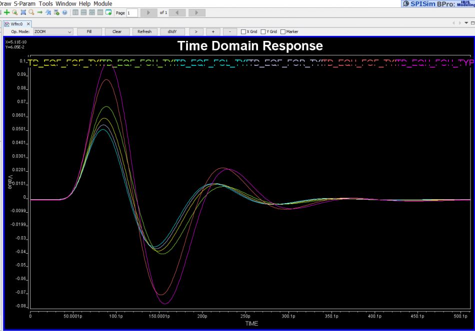
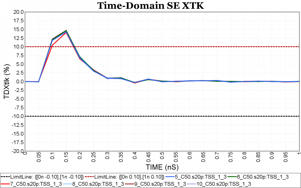
Again, one or more such time domain figures can be pre-configured so that their settings will be applied to all s-parameter data.
  • Statistics figure: The timing or skew measurement can be summarized using a histogram with distribution curve. Their data in csv format can provide more detailed info. for individual cases.

Allowing further customization such as various font size, frequency unit, grid line etc will make the generated reports more appealing aesthetically. Finally, these settings should be allowed to be imported or exported for later use. Resulting report can be in html or pdf format with indexing at the top of the page. With this kind of capability, analyzing a set of s-parameters become easy and efficient.


Report data:

When there are even more s-parameters to be processed, such as hundreds or even thousands of cases from analysis methodology such as design-of-experiment or multi-dimensional sweep, even visually check with reporting becomes time consuming. In this situation, batch processing to extract performance value, summarized in a multi-column csv fashion to be used for statistic tool such as our MPro or JMP is more practical.

User first specify all the files to be processed, then specify one or more time domain or frequency domain performance targets. The processed results can be visualized as a summary plot. Interested cases or outliers can then be selected to generate more detailed report or investigate individually.

Unless specified, all the screen captures used in this post are from our SPIPro product. All the mentioned functions and capabilities are also supported in this product.

S-Param: Quality checklist

Preface:

In a typical system, there are usually three type of models involving in simulation or analysis:

  1. IBIS/IBIS-AMI: At the both ends of the channel are driver and receiver models, usually in the forms of spice, IBIS and/or AMI.
  2. RLGC: Interconnects with homogeneous structure such as transmission line and/or layer stackup are usually 2D/2.5D field solved and represented with frequency dependent RLGC matrices
  3. S-Parameter: Complicated passive structures such as package, connector or via must be solved with full-wave simulation to have accurate representations, which are almost always S-parameter.

In the recent years, due to the popularity of link analysis for low BER requirement (i.e. various SERDES interfaces), S-parameter has become more and more important. A s-parameter is now often used to represent the full channel (package + t-line + via + connector etc). In addition, there are lab measurements from VNA which are also in the form of S-parameter. Even when behavior models (broadband spice circuit) of these components are used for time domain simulation, they are also converted originally from S-param via algorithms like rational fitting.

Each of these S-parameter may have their own noise sources, bandwidth limitation or numerical inaccuracies. As a result, one has to check the quality of the S-parameter models to avoid numerical errors or instability (e.g. simulation convergence) of the analysis at the later stages.

There have been several documents floating on the web discussing about checking list for a given S-parameter, albeit lack of systematic approach or industrial support across different vendors. For this purpose, IEEE P370 committee was formed in 2015 to discuss and define a spec. as a reference. Task group 3 of this committee focuses in particularly on the S-parameter quality check. As a participating company in this joint effort since the very beginning, also as the spec. draft is coming into shape at this moment, we think it’s a good time now to share the collective thoughts and also demonstrate how these ideas are implemented in tool like our flag ship product, SPIPro.


S-Parameter quality check:

A S-parameter checking list can usually be classified into two categories: generic check and application specific check. This post focuses on the generic check, which is defined as checking based on their physical properties. For the latter one, application specific condition such as signaling speed, typologies, modulation method or even coding are further imposed. Generally speaking, there are several generic checks need to be done:

  • Passivity: to make sure data is passive and has no amplification
  • Causality: to make sure properties of cause and consequence are maintained
  • Reciprocity: to make sure data is symmetric
  • Even/Odd/Asymptotic behavior: to make sure even and odd behaviors are maintained at both DC and high frequencies
  • Connectivity: to make sure connectivity of structure extracted is correct and has no broken link(s)

In addition, reports from all of these check should be presented clearly with an overview and further details available. The overview summary should also use a single number for each check as well as quality metric coded with color for different level:

  • Good: Green
  • Acceptable: Blue
  • Inconclusive: Yellow
  • Bad: Red
  • NA: for information only, such as connectivity

Numerical criteria for these levels depends on the types of check. Lastly, visual checks should also be used in some cases to provide frequency specific information such as where the issue happened.

Full mathematical details and explanations of the sections below will be in IEEE P370 spec.. It will be made available free to public upon completion. We will not duplicate the details here but only giving high level description and demonstration usage below.


Passivity:

Power injected into a S-parameter, which includes those from incident and reflected waves, should be preserved without amplification. When this is true, then S-parameter is passive and does not contain any energy source. Mathematical requirement is:

Visually, we can plot the given traces (Sij) and see whether they cross threshold of 1.0:

And/or compute a summarized metric, Passive Quality Metric (PQM):

reported as a single value:

One way to fix a non-passive system can be use the largest (violated) value to normalize the rest such that no value is larger than 1.0, thus passive.


Causality:

Causality check is the most important, yet more complicated one for a S-parameter. A necessary but non sufficient condition of being causal is that the even and odd function behavior of the real and imaginary data at DC should be satisfied. Adding being passive across full frequency range will make the condition sufficient. So a causality check essentially includes many of the other checks needed for a s-param.

Due to the complexity of the math, such comprehensive check is not easy. As a result, a visual check (heuristic) may be used. This check is based on the observation that a polar plot of a causal system rotates mostly clockwise and is often very smooth. The small inner circle is usually where resonant happens which may degrade the causality of the overall data:

The progress of phase between two adjacent vectors (Sf0, i, j to Sf1, i, j) can be calculated and normalized with their dot product and magnitude. The results should be a value falling between -1 ~ 1. Negative value represents decreasing group delay and thus a counter-clockwise phase change between these two vectors. This is where resonance has occurred. One can plot such measure against each frequency and got its visual representation:

Often time, through type traces of a given s-parameter (S12 or S21) are used for iFFT for corresponding pulse or impulse responses. One can calculate this for each frequency of each through through type signal and have a summarized metric: Causality Quality Metric (CQM)

And report can contain more details about violations of different frequencies:

The fix of a non-causal system usually involves reconstructing a causal system with parameters fit the given data. Vector fitting or rational approximation are such approaches, which will be discussed in future post in more details.


Reciprocity:

As a s-parameter is passive, it should not be directional regarding input and output ports. Thus a S-parameter’s content should be symmetric across the diagonal part. Note that this may not be the case for materials which has non-diagonalizable property such as ferrites, yet it should hold true for most of the materials used in system elements and materials.

For a large multi-port system, color coded cell values can be used as a visual check for symmetry (reciprocity):

This needs to be done at least at the first (low) and last (high) frequency content. Regarding an overall evaluation, a Reciprocity Quality Metric (RQM) can be used:

A reciprocity violation’s fix is usually the easiest… one may average values from both sides of diagonal and replace in place.


Even/Odd/Asymptotic behavior:

This check is based on the fact that a transfer function should be equal to its conjugate in the negative frequency domain:

As a result, the real part of the data should be an even function while the imaginary part should be an odd one. That means at the dc level, the real data should be flat across freq = 0 axis while the image should cross origin point. Also at the highest frequency, the imaginary data should approach zero. One can think of all the inductive and reactive elements such as capacitors and inductors are either open or short at the lowest (DC) and highest (infinity) frequency point, thus make the transfer function real only.

This even/odd/asymptotic behavior is very useful when the extrapolation toward DC and highest frequency points are needed, such as the case for TDR/TDT from iFFT. DC point in frequency domain will affect the corresponding DC value at the time domain, while the highest frequency available will decide the resolution in the converted data in the time domain.


Connectivity:

This is to make sure the structure the s-parameter extracted from does not contain any broken channel. A simple conversion of S-parameter to Y or Z parameter and check their value should reveal the connectivity. Usually doing so at the first data point (low frequency) is enough. Color coded matrix value again will be very useful especially for large s-parameter matrix:

The example shown above is for a full DDR byte lane which involves many DQ and a pair of DQS signals. As DQS is differential, it may also be useful to separate them from the rest of the data with proper scaling for better distinction.


Report and summary:

To apply these checks to more than one  s-parameter, a batch mode process is often preferred and will save lots of mouse clickings:

The produced summary should contain with color coded cell and various quality metric number, plus further details for each check of different data. This will certainly gives user better idea about the quality of their s-parameter files.

All the screen captures used in this post are from our SPIPro product, which also implemented all the checks according to the IEEE P370 spec. draft.


Optimization for PI: Layout synthesis & Cap selections

In system analysis, signal integrity is done in either pre-layout and post-layout phase. Power integrity (PI), on the other hand, deals with mostly post-layout data. Layout is usually generated manually and then simulated in time consuming 3D solving process. As a result, optimization flow for PI is quite different from that for SI and is also very problem specific.

Power Integrity:

Power delivery model

Power delivery model

Power integrity aims at providing “clean” voltage supply to active elements in the channel such as driver and receiver. A typical representation of power delivery network is shown above, it starts with the voltage regulation and includes the motherboard, the package, and the die itself. Due to the impedance associated with the power delivery loop, any current through this loop will cause a drop in the voltage available to the die. Current is supplied from voltage regulator ultimately but is also stored in the de-coupling capacitors on the conducting path.This drawing current (Icct or Iload) varies due to different number of buffers switching at different frequency or work load… This drop in the voltage at the die directly impacts the maximum operating frequency of the design. Thus a spec. must be provided and met for the droop voltage to assure design quality.

The impedance in the power delivery loop can be classified as both resistive and inductive. The resistive drop is proportional to the current through the loop while the inductive drop is proportional to the rate of change of current. It is desired to have small loop inductance as Ldi/dt will contribute to the droop. This inductive drop is typically countered by adding several stages of decoupling caps at various points in the power delivery network. This helps reduce the overall impedance of the power delivery loop over a broad frequency range.

The conducting paths are layout design, rather than spice-like electrical netlist. The decoupling caps are usually provided by external vendors (e.g. Murata) and the designer needs to decide where and how to place them. So a power integrity analysis usually includes the following aspects:

  • stackup, power via arrangement and pin out;
  • decoupling strategy, choice of location, number and value of caps

Optimization w/ Design synthesis:

The power delivery network is layout design solved with 3D field solver. If designs can be generated via rule-based synthesis, then the design cycle can be shortened and many designs can be generated in advance. A batch-mode like process is then used to solve for different PDN models for comparison and trade-off study.

antenna

Take the different on-chip antennas shown above as an example, they are specified with different geometry parameters so that software algorithms is used to synthesize the design quickly. Do so manually may not be accurate or efficient. For a PD design, the rules are much more complicated than just the geometrical based parameters. Nevertheless, best practice or experienced based rules can still be summarized so that algorithm can perform the following tasks automcatically:

  • Modify layer stackup thickness and material properties
  • Generate pin, nodes, traces and shapes on specific layer either based on net name or reference location to other (signal or power) pins
  • Generate (power) vias in certain pattern and connect to power/ground planes. Voids and proper pad-stacks are also generated as part of the process
  • Duplicate certain region of the design (template) to other area as a X-Y array
  • Perform DRC alone the way and generate warnings

The flow mentioned above is purposely built for a certain solver, it’s because different solver has its own definitions for different design object (via, traces, nodes etc) and the layout syntax is also solver specific. Nevertheless, this flow has great potential of shorten design cycle, permit design optimization via quick analysis of different design, and even reduce the needs for engineering layout resources.

Decoupling analysis:

Once decoupling strategy (land side caps and/or die-side caps) and corresponding layout is generated, a S-parameter for the PDN can be obtained via 3D field solving. With proper provision (not stuffing cap in advance in the design), this generated S-parameter may be used directly again and again for what-if decoupling analysis. If there is no layout/stackup change, 3D solving does not need to be repeated.

CapEff

As shown above, different combination of caps “stuffed” at the output ports will cause impedance seeing into the die ports to vary. Conceptually, one may simulate the given S-parameter with cap connected and measure the impedance using simulation in frequency domain. In practice, such simulation is not needed as S-parameter can be converted into Y/Z-parameters and lumped together with cap’s FD impedance and be analyzed directly. As a result, we can post-process the PDN’s S-parameter for a certain decoupling cap arrangement to gain the following insights very quickly:

  • The impedance (both inductive and resistive) of the PDNLac
  • Current contributed by each de-caps at certain frequencyZIAC
  • Input impedance seen at each die-portZf
  • Effective analysis: by removing a particular de-cap, how much impact does it have to the die’s impedance.ZFCIF
  • How does this compare to different configuration: repeat the same “what-if” analysis for different configuration.