
Most parts of the channel between driver and receiver, usually in the form of multi-segment transmission lines connected together or through different vias, reside on different layers of PCB. Thus it’s important to understand how these layers and transmission lines are modeled for signal/power integrity analysis.
Layer stackup:
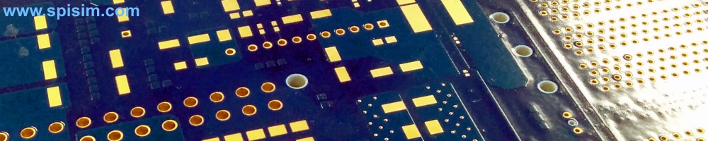
A print circuit board (PCB) is usually composed of multiple layers in a modern system. Several sheets of cooper wrapped cores are bonded together with pre-preg in between to form multiple layers. The core and pre-preg are dielectric materials and coppers serve as medium of conducting plane and traces. Copper’s height is often represented by weight in terms of oz, and dielectric is made off lame retardant material (FR4). Depending on the number of routing and plane layers needed, common PCBs are often 6, 8, and 10 layers for desktop or mobile application. Both material and geometry properties of stackup and traces are quite homogeneous and can be simulated with 2D field solver.
Different conducting layers are connected with “via”, which is a barrel of conducting plate and pads/anti-pads at different layers. There are several different types of vias: PTH for plate through hole from top to bottom layers, blind layers (originates from top or bottom and ends at inner layer) and buried via. Via structures are usually non-uniform and require 3D field solver to model, thus is not included in the discussion in the layer/transmission line context.
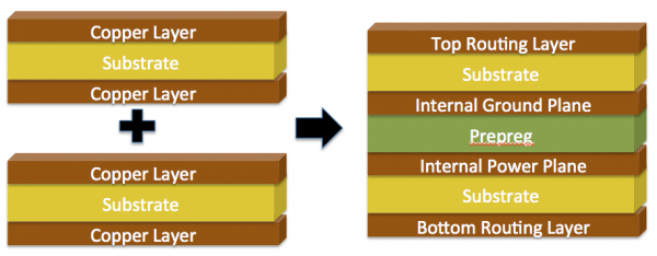
Layers of copper+core are bonded together…
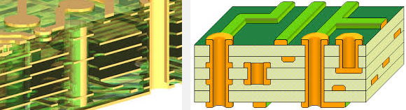
Different types of vias
Transmission line (T-Line):
Some of the conducting layers in the multi-layer PCB are used for signal traces routing. Depending on which layer they are, different relations respect to the adjacent reference plane may be formed: Microstrip, Stripline and Dual stripline.
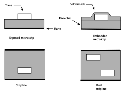
Types of traces
In terms of circuit modeling, each short segment of such traces can be represented as a RLGC lumped element. The values of R/L/G/C depends on the cooper conductivity, surrounding dielectric’s permittivity, loss tangent and trace’s geometric properties such as width, height and distance to the reference plan. When propagation time through such small segment is longer than one tenth of the signal rise time, then lumped model is no longer valid. One must use Maxwell equations to explain the signal propagation behavior along this signal trace. Having that said, the circuit model of non-lumped transmission line is still represented by R/L/G/C values or matrices solved by field solver with aforementioned material and geometrical properties according to the Maxwell equations.
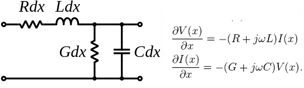
Lumped model and T-Line equation
T-Line performance parameters:
Several performance parameters can be defined based on a T-Line’s R/L/G/C model to describe its properties:
- Impedance: Energy may be partially reflected at the boundary where impedance becomes discontinuous or mismatched. This is one of dominate factors in signal integrity problems called inter-symbol interference (ISI). Thus a quick scan of characteristic impedance of signal traces along the path can reveal many useful information why signal deteriorates.
- Crosstalk: While diagonal terms of R/L/G/C matrices explains the relationship of trace itself to the reference plan, the off-diagonal portion explains the interactions between different traces. The energy is shared between these traces because of the EM fields and thus a nearby aggressor can often cause victim’s signal integrity problem particular when they run in parallel for very long distance.
- Propagation delay and attenuation: These are often secondary factors when comparing to impedance and crosstalk. Signal of different frequencies propagate at different speed and suffer from different degrees of attenuation, both contribute to the deterioration of signal.

Extract performance parameters from a T-Line’s model
Stackup and T-Line modeling:
There are often trade-offs between layer stackup and routing T-Line when designing a system. For example, the PCB cost is reduced with fewer layer count yet dense routing or narrow trace width may incur more crosstalk or higher impedance. Also, how to plan trace geometries to make sure impedance is well matched along the channel? All these may need detailed planning in advance before traces or components are lay out. Thus the purpose of stackup and T-Line modeling is to explore the relationship of costs (in terms of layer count or dimensions etc) vs trace performances.
As both material and geometrical properties comes into play, on top of different trace type (microstip, strip-line etc), there are many factors to consider and one needs to identify primary ones vs performance. Basic steps may include:
- Decide layer counts and where the traces will be routed
- Decide material and geometry variables for the layers and traces
- Generate a simulation plan to sweep across these parameters
- Execute the sweep plan using field solver and obtain traces’ RLGC models
- Extract performance parameters and map input variables to these targets
- Identify whether this mapping (prediction model) contains desired solution
- Go to step one and try different layer configuration if needed.

Layer and trace modeling
If the layer configuration is used often, one may also record the mapping model as prediction formula for future use. Our experience has shown that such models usually do not require higher order (>2) terms and are very well behaved for prediction purpose.
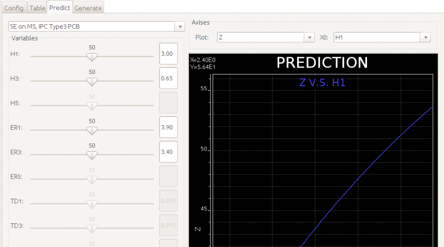
Prediction model