IBIS model: How does IBIS work

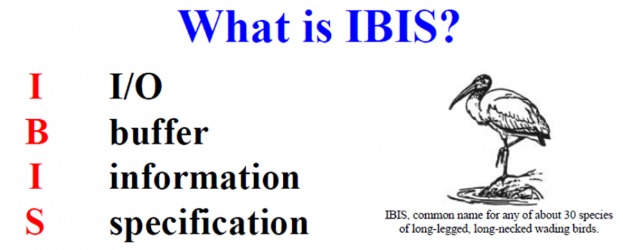
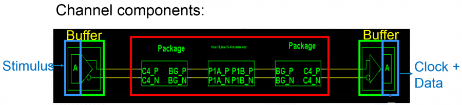
* Buffer model: What is in an IBIS model:

IBISType

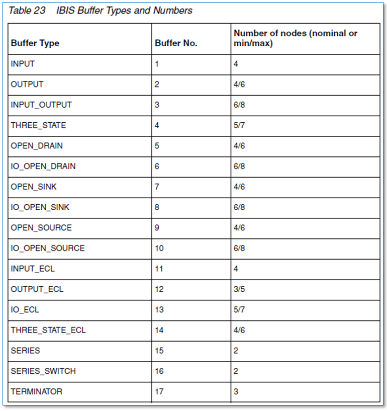
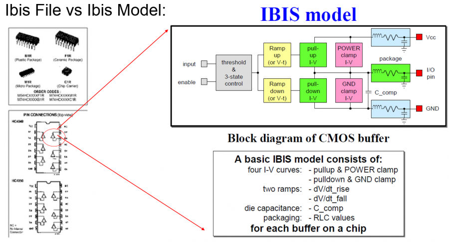
IBIS Spec defines many different buffer model types, as shown above. Different model types requires different modeling data to be included in the IBIS model section. In general, an IBIS model will have the following info.

  • Operational conditions: such as voltage and temperature range for operations
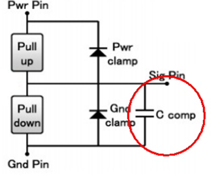
  • Parasitics/Loading conditions: such as C_Comp of the model. This value does not impact buffer performance when output is well terminated.
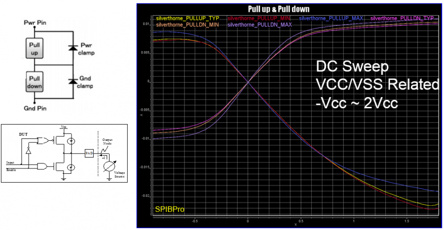
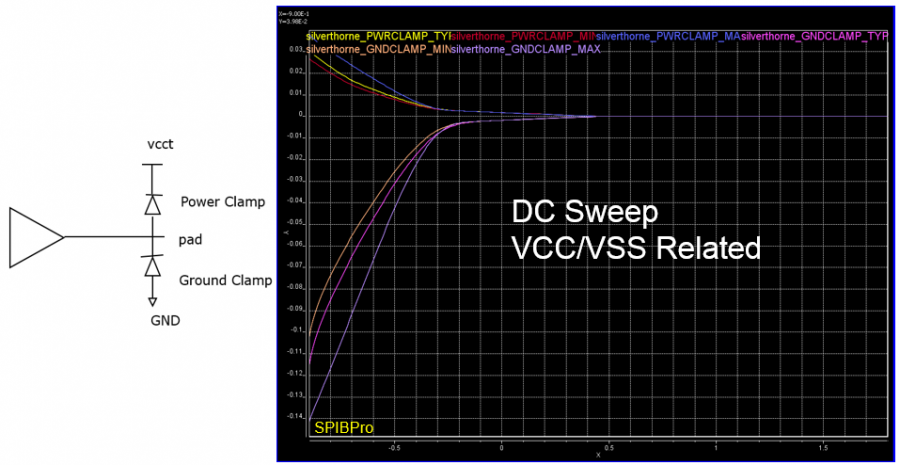
  • I/V table: These are I vs V tables of different corners for pull-up (PU), pull-down (PD), power clamp (PC) and ground clmap (GC) circuitry. They are general representations of non-linear resistor like those E elements used in the hspice circuit. According to the spec, the sweep range for these table should be from -Vcc to 2Vcc where Vcc is the power supply voltage. The reason is that in case of total reflection from the far side of the loss-less channel, either to do fully open or fully connected to ground, added full Vcc voltage swing will extend the original 0 ~ Vcc range to -Vcc to 2Vcc. Also notice that for IV sweep of pull-up circuitry, i.e. PU and PC, the voltage is Vcc relative. That means value of I when V = 0 is actually when V = 0 to Vcc = Vcc to ground. One usually needs to make such conversion back to be VSS relative during debugging process. SPISim’s IBIS module, SPIBPro, has such a GUI button to translate Vcc relative to Vss relative waveform directly.
    IBISPUPD
    IBISPCGC
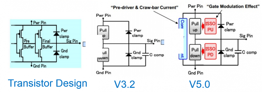
  • ISSO PU/PD: These are current tables introduced in V5.0, used when terminal VCC and VSS voltages are not ideal. With lower VCC voltage due to PDN network (i.e. voltage droop), buffer strength will become weaker. So are those caused by ground bounce. This phenomena is usually called “Gate modulation effect”. ISSO/PU and PD data defines the effective current of the pull-up/pull-down structures as a function of the voltage on the pull-up/pull-down reference nodes (ideal is Vcc and Vss/Gnd)
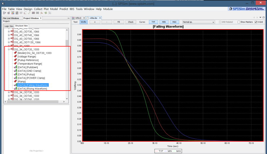
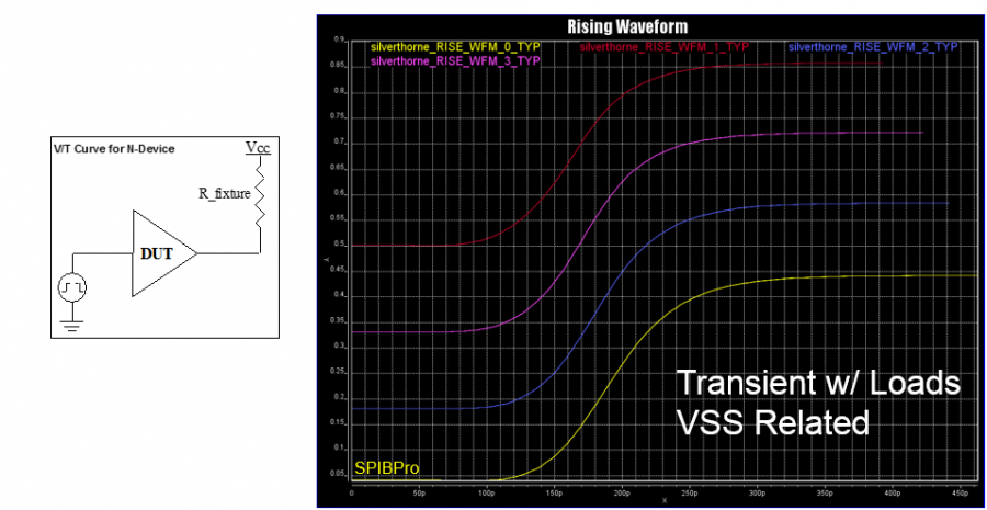
  • V/T table: These are tables representing buffer’s voltage at die output vs elapsed buffer switching time. Under different loading condition, such as test load and test fixture, resulting waveform will be different. An ibis model usually will include at least two such VT tables under different loading condition to provide sufficient coverage during real world operations.
    IBISVT
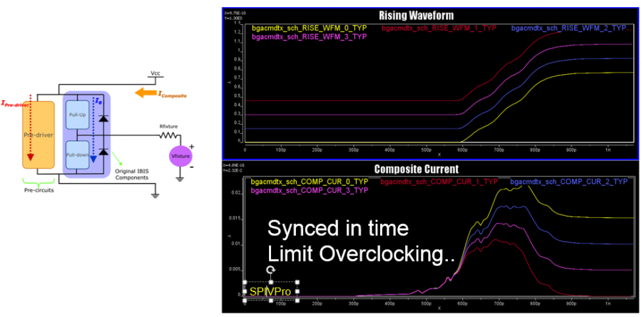
  • I/T table: These are tables representing buffer’s drawing current vs elapsed buffer switching time. It needs to be synchronized with aforementioned VT table so that current drawn happens at the exactly same time point for the same test fixture. This current is usually composed of bypass current, pre-driver current crow-bar current and termination current if present.
    IBISIT

* How is IBIS modeling data used during circuit simulation:
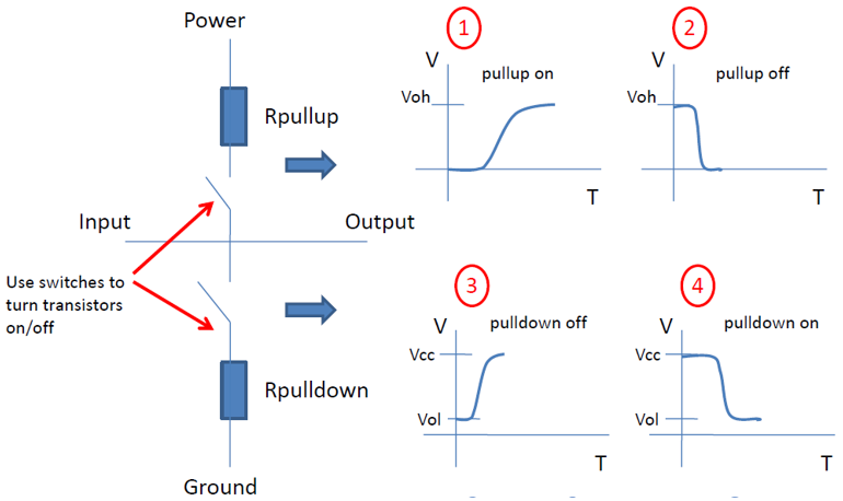
With so many tables, one may wonder how they are used in a circuit simulator. To simplify, let’s first remove the ESD protection circuitry PC and GC as they are usually reversed biased and contribute very small amount of current. For the remain PU and PD circuitry, we can imagine them as non-linear resistors, similar to those MOSFET’s channel resistance when terminal voltages varies. How these two table work together during different loading condition decide the resulting transient VT waveform shown in the VT/IT table.
IBISKuKd0

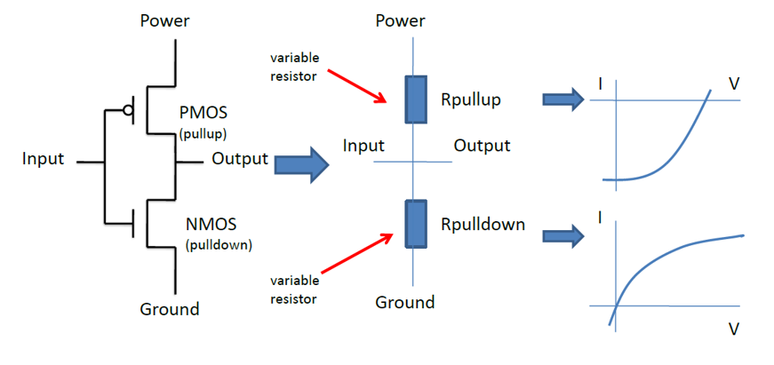
During rising transition, PU circuitry gradually turns to fully ON while PD circuit gradually turns to fully OFF. Similarly, during falling transition, PU gradually turns to fully OFF and PD turns ON. Thus we can define a time dependent parameter, “switching coefficient”, which will be applied to PU and PD separately such that the resulting current from these two branches mimic the gradually turning ON/OFF effect.
IBISKuKd1

Let’s call these two switching parameters Ku(t) and Kd(t). We needs two equations to solve these two unknowns. Now assuming we have to such VT table under different loading condition. At each time point of these two tables, we know the loading condition and instant output voltage of the buffer. Using these, we can solve Ku(t) and Kd(t) in which the time, t, is buffer switched elapsed time. That is, the x-axis of the VT table.

If we don’t have two waveform table, one may make an assumption that Ku(t) + Kd(t) = 1 at all times. This is usually true at the static high or static low output condition but may not be in between. One may also use ramp parameters in the IBIS model to generate an artificial VT table for the same purpose.
IBISKuKd2

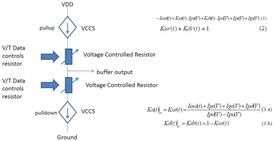
For an IBIS model developer for circuit simulator, he/she needs to consider all the branch current to obtain accurate Ku(t), Kd(t) solutions. So reverse bias current from ESD circuit need to be put in and so is the current flowing through C_Comp. For example, i=C_Comp * dV/dt can be sued to subtract current flow through this capacitor from the total output current and avoid double counting.

IBISCComp

For power-aware model, another level of scaling parameter needs to be applied. These new parameter need to scale the buffer output strength based on the instant nodal voltages across buffer terminals such that gate modulation effect will be taken into account.

Interested reader may find detailed algorithm in the following two paper.

IBIS model: What is IBIS

IBIS is short of I/O Buffer Information Specification. The spec. was proposed in early 90’s to promote tool independent I/O models for system level analysis. It’s been evolved since even until this date. It’s now an ANSI standard and are widely supported by different system level EDA vendors, including SPISim.

IBISLogo
IBIS model is created as a behavoiral model for transistor’s buffer deisgn used in system level analysis. Several milestones and its delta improvements have been listed briefly below:

  • Version 3.2, using IV/VT data table to address and meet most signal integrity’s needs.
  • Version 4.0, introduces other language such as Verilog-A, VHDL and Berkeley spice as external circuits to address shortcomings of rigid IBIS syntax, which often is not flexible enough to represent behaviors more advanced buffer design.
  • Version 5.0 introduces power aware features. By introducing ISSO PU/PD and Composite Current which represents currents drawn from power delivery network (PDN), the voltage droop and ground bounce issues during simultaneous switching can be modeled and analyzed.
  • Version 5.1 introduce AMI to account for equalization mechanism which sits transmitter’s analog front end and behind receiver’s buffer output. AMI model is mostly written in C/C++ compiled into .Dll or .so loaded by simulator. This deviation from more high level language such as Verilog-A gave model designers tremendous flexibility in modeling the full EQ + buffer to enable bit-error-rate based analysis. However, it also significantly increase the barriers and difficulties to create a good buffer model.

IBISEvolve

When talking about the term “IBIS””, one needs to distinguish about IBIS Spec, an IBIS file and a IBIS model. The following list gives simple overview:

  • IBIS Spec: Spec. defined by IBIS committee. In addition to the buffer related portion, its general meanings may also include connector spec (ICM, InterConnect modeling Spec). ICM provides standard model format for all electrical interconnects such as cables, connectors, package and printed PCB. Previously, a different spec, EBD… electric board description was used. ICM is to replace EBD.
  • IBIS File: An IBIS file is like a container of models for an IC or chipset. An IC package usually has many pins, with several buffers inside. Thus an IBIS file usually have manufacturer’s info as part of the headers, followed by different pins, pin names and connected buffers, then detailed various buffer models and their modeling data. An IBIS file may also have package models and AMI statements which points to associated .ami and .dll/.so files for corresponding equalizer portion of the design.
  • IBIS Model: An IBIS model is an individual buffer model sits inside the IBIS file. Depending on modeling type and the IBIS version, it may have I/T, V/T, I/V data tables and corresponding operation and loading condition when these model are being excited for modeling. It’s desired the usage of this buffer model should not deviate from the modeling condition too much as the behavior in those range may not cover properly in the constructed model.
IBIS Files vs Models

IBIS Files vs Models

Viewing model data of an IBIS file in SPIBPro

Viewing model data of an IBIS file in SPIBPro

IBIS model: What is buffer model and why IBIS

Before we are going to dive into details about buffer model, we need talk about why we care…

Buffers sit at the driving and receiving ends of a channel. So while the passive channel is composed of models like transmission lines, vias and connectors, the models sit at both ends are buffer.
Channel
If you are a circuit designer, in particular, a chipset designer, you pay attentions to the transistor sizing and the associated process, voltage and temperature corners (so called PVT corners) so that you will be assure that the designed buffer, when connected to the system, will have desired strength, impedance and timing.

Transistor and process info. for a buffer design

Transistor and process info. for a buffer design

However, if you are a system designer, or a signal integrity engineer. You pay attentions to higher level of the system design, such as component placement, routing, topology, termination etc. A buffer or an IC to you is just a component off the shelf. Those design details like transistor sizing, silicon doping concentration etc are too much details for you and are mostly not needed to what you are doing. Just like when software designer make connections between libraries, they make use of application interface (API). A much simplified model to represent these buffers are thus needed to enable system design.

Thus from the perspective of needs to interface between transistor level and system level design, a behavioral model representing a buffer is certainly needed.

System level design use buffer as component.

System level design use buffer as component.

Now when we talk about buffer modeling, there are several requirements derived from different perspectives:
A good buffer model needs to be:

  • Accurate: This is most important consideration. Garbage in, garbage out. By accurate, it’s usually considered to be within 5% tolerance of corresponding original, transistor design.
  • Protect IP: From IC/Chip set manufacturer’s perspective, they release buffer model mostly publicly to enable their customers adopt the design. However, they also do not want to reveal any IP such as how the buffer is designed and the manufacturing process info.
  • Run very fast: From system designer’s view, a buffer needs to run very fast, typically at 100X ~ 1000X of the corresponding transistor design. Only so then system design, which usually includes hundreds’ or even thousands’ of buffer, is made possible.
  • Easy to generate: For a model generation engineer’s perspective, if it takes lots of effort to generate and correlate the buffer model from its transistor counterparts, then the model generation process will become error prone and cause accuracy concern. Black-box type modeling is desired mostly as the model generation engineer does not need to know how these buffers are designed yet he/she can still generate buffer model which matches its original transistor’s performance.
  • Follow industry standard: A good buffer model should follow industrial spec. or format such that it can be simulated with different vendor’s tool, such as Synopsis’s Hspice, Cadence’s SystemSI or Agilent’s ADS. A model locked in to a particular tool is usually just to hide potential accuracy and easy generation issues down the road.Often in such considerations, one may consider using encrypted transistor netlist, such as encrypted Hspice, for model release. However, this will defeat the requirement of speedy simulation performance as encrypted model is usually run at the same speed of their transistor originals.From these considerations, several industrial standard have been proposed and widely used for buffer modeling used in system level analysis. They includes: IBIS and Verilog-A. In which, IBIS is most widely used and has been around since mid 1990. More info. about IBIS spec can be obtained from the ANSI’s IBIS website [HERE].

What is a system:

System integrities include signal integrity (SI), power integrity (PI) and electro-magnetic compatibilities (EMC) in general. They are analyzed via circuit modeling and simulations. However, what is the scope of a system?

20120126_01

Fig.1 is a typical pc mainboard we usually see. There are many components, such as heat sinks, various capacitors and connectors on the board’s top layer. When flipped over, we also see that there are many solder points and routing traces like Fig. 2. System like this is the scope of our analysis. Note that it doesn’t have to be a PC system… mobile phone, embedded devices or even high-end server are also treated the same. They are just different in terms of circuit size and scale.


20120126_02

These systems are designed with CAD software (Fig. 3) When we zoom in part of the schematic, we will find many routing traces extended from the chip’s pins’ locations to the edge of the board… usually where the connectors are located. (Fig. 4)


20120126_03

If we further zoom in to the edges around these chip’s pins, and visually in a 3D view (Fig. 5), One may see that there are many vertical cylinders making transitions between different layers. As a package and sometimes sockets sit between silicon chip and underlying mainboard, and a system board is also mostly composed of more than top and bottom layers. These cylinders are called “Via”. A cross-section view makes these via transitions more clear. Conducting traces are extended outwards like roads carrying electrons leaving the central hub.


20120126_04

Moving upstream toward inside the chip, we will be marching into the silicon world where designs are mostly realized with MOSFETs. Logics are computed and bits/bytes are stored here. Signals are eventually buffered and amplified before sending out to pass through aforementioned vias, traces, capacitors, connectors and finally reach the end of path.. receiver.


System Modeling:

From these simple illustrations above, one can see that in order to analyze a system’s performance, the following involved factors must be studied and modeled for simulation:

  • Driver/Receiver: How to create and simulate transistor buffers. Topics include IBIS and AMS modeling etc.
  • Packaging: Type of packaging and how to model etc.
  • PC board: How to model and analyze different layer stack-ups. How does the dielectric medium and conductors affect the signaling etc.
  • Trace (Transmission line): how to plan, model and analyze their cross talks etc.
  • Via/Connector: How to create such model, and analyze their performance.
  • Channel: How to assemble the individual elements above together as a channel and perform circuit analysis.
  • Signal: Signal for different interfaces (PCIe, DDR etc), signaling (single-ended and differential) and encoding etc.

In the subsequent topics, we plan to walk through the modeling and analysis practices for these system elements.

Preface

About SPISim blog:

SPISim TM focuses on signal, power integrity and simulation. Our products are realization of the methodologies, flows and algorithms as EDA software in these domains. To further share our design concepts, common practices and knowledge in SI, PI and simulation areas, we think blog articles are necessary and will be beneficial.

Our blogs intends to achieve the following goals:

  • To serve as our central repository for fundamentals and advanced knowledge in SI, PI and simulation areas;
  • To serve as a channel to advocate our software design concept, common practices and analysis ideas;
  • To collect comments and feedbacks from readers for our products’ new features considerations.

We plan to publish blog articles several times a week to cover the following topics:

  • Fundamentals: e.g. SI, PI basic concepts;
  • Modeling: e.g. transmission line, s-parameter or driver modeling;
  • Analysis: e.g. jitter, noise or timing analysis;
  • Methodologies: e.g. responsive surface modeling, peak distortion analysis;
  • Simulation: e.g. how these devices/algorithms are put together for circuit simulation;
  • Software: e.g. realization of the topics above into our SPISim products.