IBIS-AMI: An end-to-end AMI modeling flow

In previous post, I mentioned about the “IBIS cook-book” as a good reference for the analog portion of the buffer modeling. Unfortunately, when it comes to the equalization part, i.e. AMI, there is no similar counterpart AFAIK. For the AMI modeling, the EQ algorithms need to be realized with algorithms/procedures implemented as spec. compliant APIs and written in C language. These functions then need to be compiled as a dynamic library in either dynamic link libraries (.dll on windows) or “shared objects (.so on linux-like). Different compiler and build tool has different ways to create such files. So it’s fair to say that many of these aspects are actually in the computer science/programming domains which are outside the electrical or modeling scopes. It is unlikely to have a document to detail all these processes step-by-step.

In this post, instead of writing those “programming” details, I would like to give a high-level overview about what different steps of the AMI modeling process are… from end to end.  Briefly, they can be arranged in the following steps based on execution order:

  1. Analog modeling
  2. Prepare collateral
  3. Define architecture
  4. Create models
  5. Model validation
  6. Channel correlation
  7. Documentation

The following sections will describe each part in details.

Analog modeling:

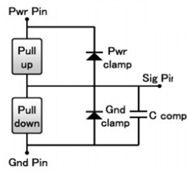
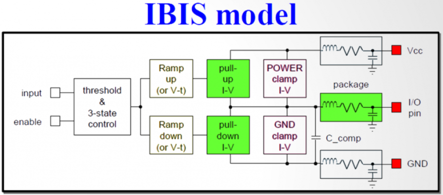
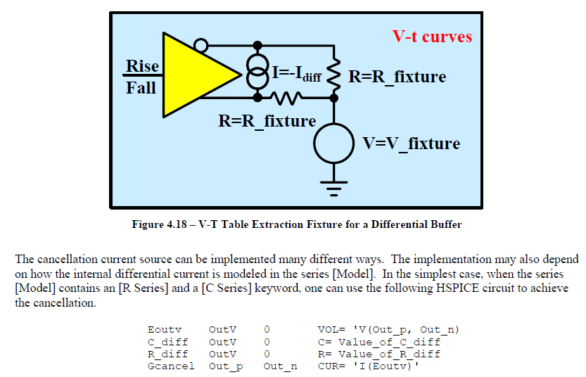
Believe it or not, the first step of AMI modeling is to create proper IBIS models… i.e. its analog portion. This is particular true if circuit being modeled belongs to TX. A TX AMI model is equalizing signals which includes its own analog buffer’s effect measured at the TX pad. So if there is no channel (pass-through) and it’s under nominal loading condition, the analog response of the TX will be the signals to be equalized. That is to say, without knowing what will be equalized (i.e. what the model’s analog behavior is), one can’t calculate the TX AMI model’s EQ parameters.

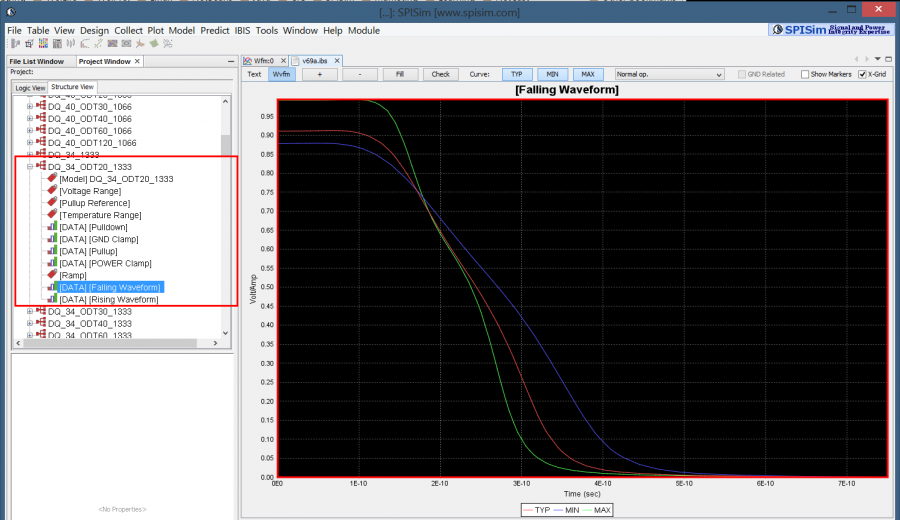
Take the plot above as an example. This is a FFE EQ circuit. The flat lines indicated by two yellow arrows are different de-emphasis settings, thus controlled by AMI. However, the rising/falling slew rate, wave shape and dc levels etc as circled in red are all analog behaviors. Thus an accurate IBIS model must be created first to establish the base lines for equalization. Recently, BIRD 194 has been proposed to use touch-stone file in lieu of an IBIS model… still the analog model must be there.

For a RX circuit, it may be easier as an input buffer is usually just a ESD clamp or terminator. Thus it doesn’t take much effort to create the IBIS model. Interested people may see my previous posts regarding various IBIS modeling topics.

Prepare collateral:

AMI’s data can be obtained from different sources: circuit simulation, lab/silicon measurement or data sheet. For simulation case, simulation must be done and the resulting waveform’s performance needs to be extracted. These values will serve as a “design targets” based on whitch AMI model’s parameters are being tuned.

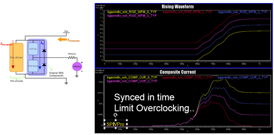
For example, this is a typical TX waveform and measured data:

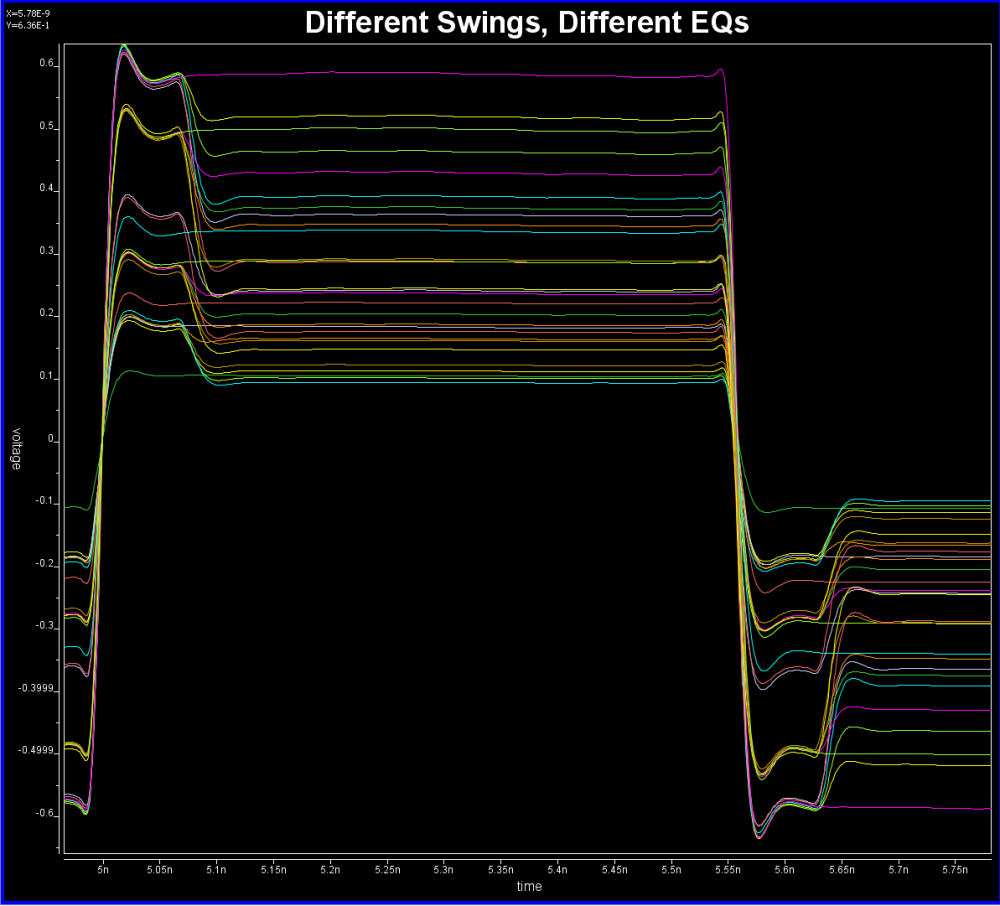
Various curves have been “lined-up” for easy post-processing. Using our VPro, we batch measured the value at the 5.3ns for different curves and created a table:
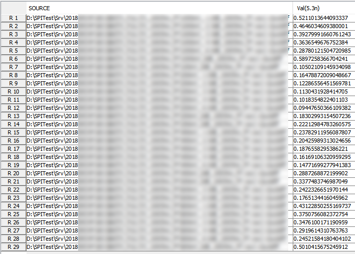
Similarly, data collected from measurement needs to be quantified. This may be done manually and maybe labor intensive as the noise is usually there:

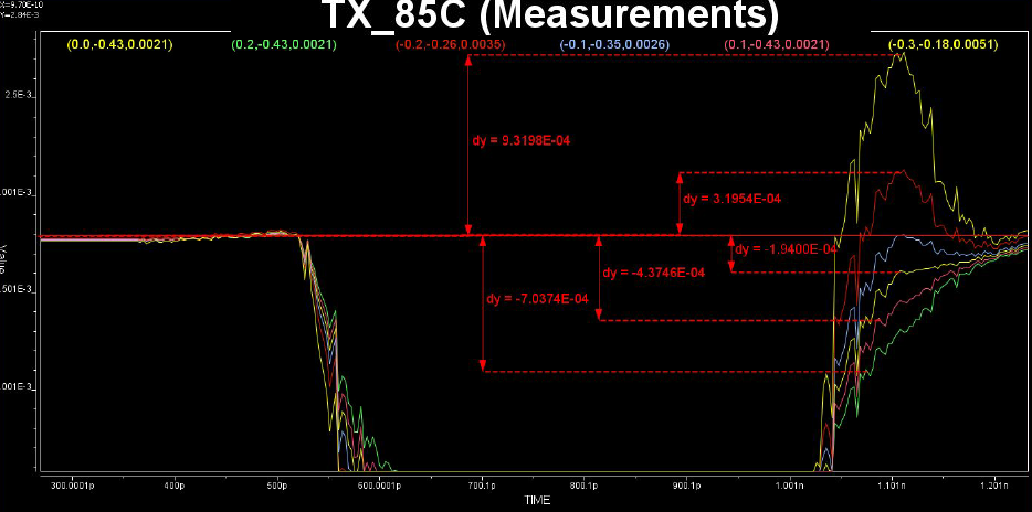
Some of the circuits may have response is in frequency domain. In this case, various points (DC, fundamental freq. 2X fundamental etc) needs to be measured like above.

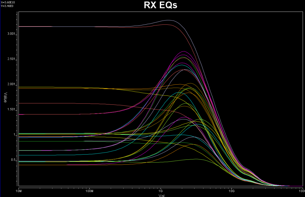
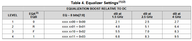
If it’s from data sheet, then the values are already there yet there may be different ways to realize such performance. For example, equations of different zeros and poles locations may all have same DC gain or gain at particular frequencies, so which one to pick may depending on other factors.

Define architecture:

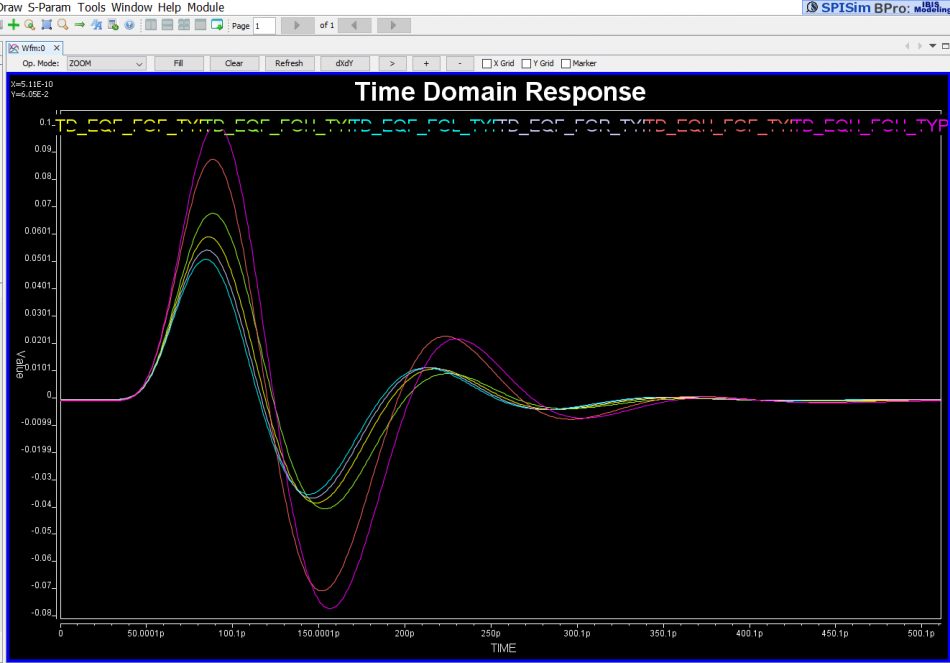
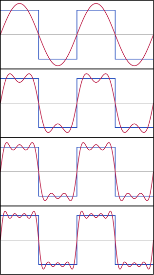
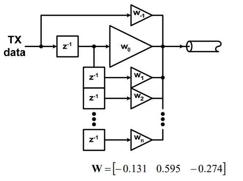
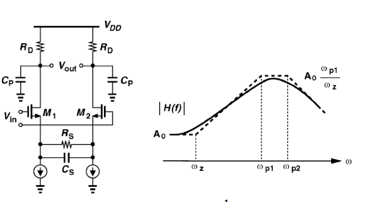
Based on the collateral and the data sheet, the modeler needs to determine how the AMI models will be built. Usually it should reflect the IC’s design functions so there are not much ambiguity here. For example, if the Rx circuit has DFE/CDR functions, then the AMI models must also contain such modules. On the other hand, some data my be represented in different ways and proper judgement needs to be made. Take this waveform as an example:

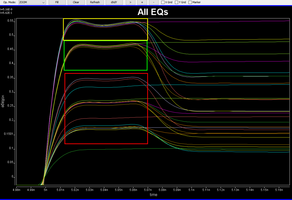
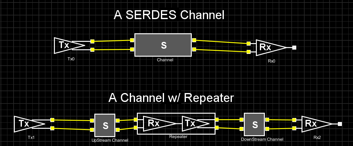
It’s already very obvious that it has a FFE with one post-tap. However, since the analog behavior needs to be represented by an IBIS model, then one needs to decide how these different behaviors, boxed in different colors, should be modeled. They can be constructed with several different IBIS models or a single IBIS model yet with some “scaling” block included so that IBIS of similar wave shapes can be squeezed or stretched. For a repeater, oftentimes people only care about what goes into and what comes out of this AMI model. The abilities to “probe” signals between a repeater’s RX and TX may be limited by the capabilities of simulator used. As a result, a modeler may have freedom determining which functions go into Rx and which go to Tx. In some cases, same model yet with different architecture needs to be created to meet different usage scenarios. An example has been discussed in our previous post [HERE]

Create models:

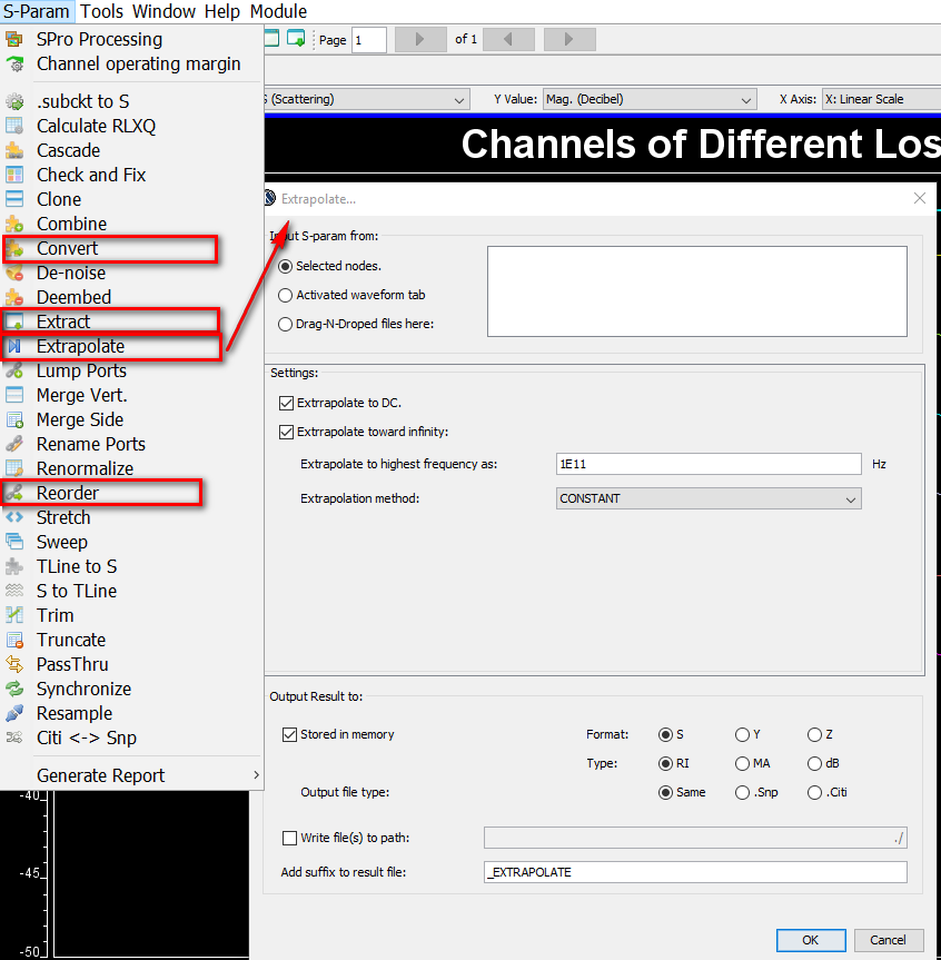
Once architecture is defined, next step is the actual C/C++ implementation. This is where programming part starts. Ideally, building blocks from previous projects are there already or will be created as a module so that they can be reused in the future. Multiple instance of the same models may be loaded together in some cases so the usage of “static” variables or function need to be very careful. Good programming practice comes into play here. I have seen models only work with certain bit-rate and 32 samples per UI. That indicates the model is “hard-coded”… it does not have codes to up-sample or down-sample the data based on the sampling-interval passed in from the API function. Accompanied with writing model’s C codes are unit testing, source revision control, compilations and dependencies check etc. The last one is particular important on linux as if your model relies on some external libraries and it is not linked statically, the same model running fine on developer’s machine will not even pass golden checker at user’s end…. because the library is not available there. Typically one will need to prepare several machines, virtual or not, which are “fresh” from OS installation and are the oldest “distros” one is willing to support. All these are typical software development process being applied toward this AMI modeling scope.

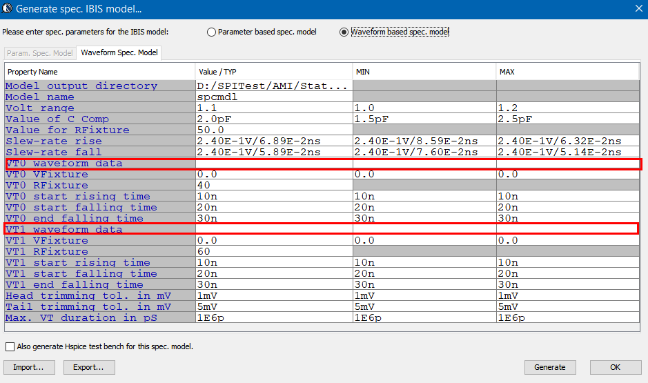
After the binary .dll/.so files are generated, then next step is to assemble a proper .ami files. Depending on parameter types (integer, values, corners etc), different flavors of syntax are available to create such file. In addition, different EDA simulators has different ways to present the parameter selections to its end user. So one may need to choose best syntax so that choices of parameter values will always be selected properly in targeted simulators. For example, if one already select TYP/MIN/MAX corner for the IBIS model, he/she should not have to do so again for the AMI part. It doesn’t make sense at all if a MIN AMI model will be used with MAX corner IBIS model… the corner should be “synchronized”.

Once the model is ready, next step is to tune the parameters so that each of the performance target will be matched. Some interface, such as PCIe, has pre-defined FFE tap weights so there are no ambiguities. In most cases, one need to find the parameter’s values to match measured or simulated performance. Such tasks is very tedious and error prone if doing manually and process like our “AutoTune” will come very handy:

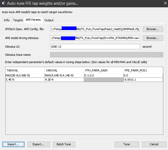
Basically, our tool let user specify matching target and tool will use bisection algorithm to find the tap values. Hundred of cases can be “tuned” in a matter of minutes. In some other cases, grid search may be needed.

Model validation:

Just like traditional IBIS, the first step of model validation is to run it through golden checker. However, one needs to do so on different platforms:

The golden checker didn’t start checking the included AMI binary models until quite recently. Basically it loads the .ibs file, identifies models with AMI functions, then check the .ami file syntax. Finally, the checker will load the associated .dll/.so files. Due to the fact that different OS platform loads binary files differently, that means certain models (e.g. .dll) can only be checked on associated platform (e.g. Windows). That’s why one needs to perform the same check on different platforms to make sure they are all successful. Library dependencies or platform issues can be identified quickly here. However, the golden checker will not drive the binary file. So the functional checks described in next paragraph will be next step.

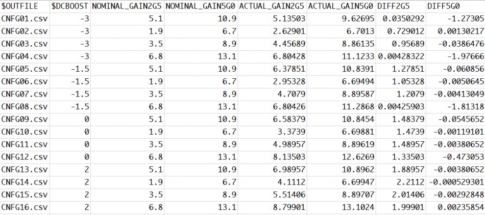
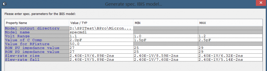
Typically, an AMI model have several parameters. To validate a model thoroughly, all combinations of these parameters values need to be exercised. We can “parameterize” settings in a .ami file like below:

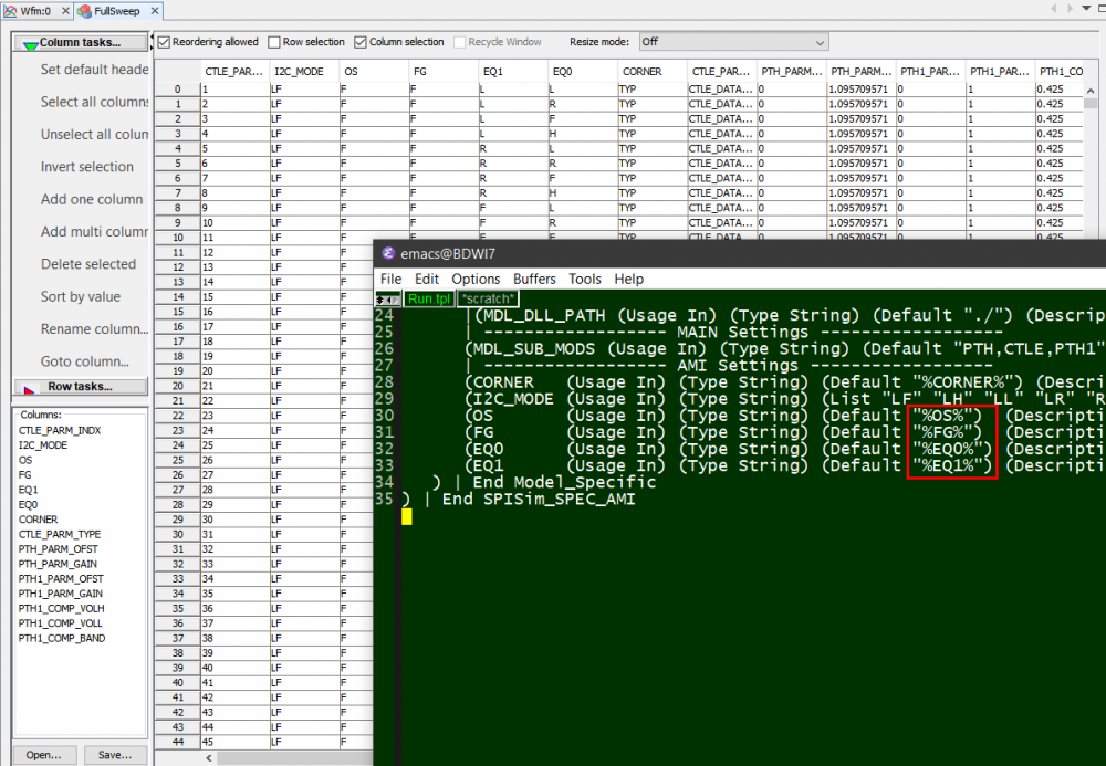
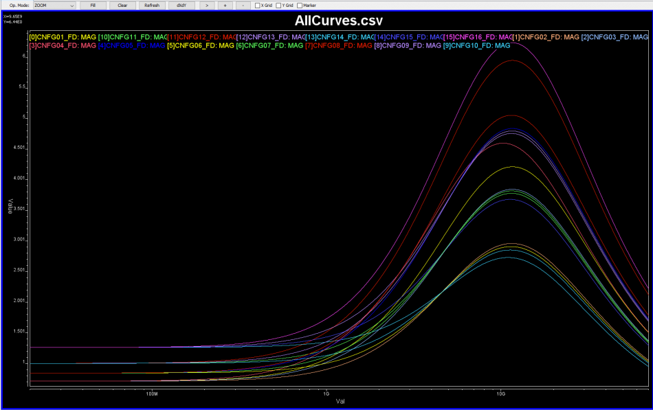
Here, pattern like %VARIABLE_NAME% is used to create a .ami template. Then our SPIMPro can be used to generate all combinations of possible parameter values and create as a table. There can usually be hundreds or even thousands cases. Similar to the process described in “Systematic approach mentioned in my previous post”, we can then generate corresponding .ami files for all these cases. So there will be hundreds or thousands of them! Next step is to be able to “drive” them and obtain single model’s performance. Depending on the EDA tools, most of them either do not have automation capability to do this in batch mode or may require further programming. In our case, our SPIMPro and SPIVPro have built-in functions to support this sweeping flow in batch mode all in the same environment. SPISimAMI model driver is used extensively here! Once each case’s simulation is done, again one needs to extract the performance then compare with those obtained from raw data and make delta comparison.

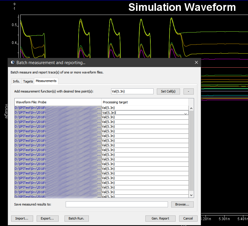
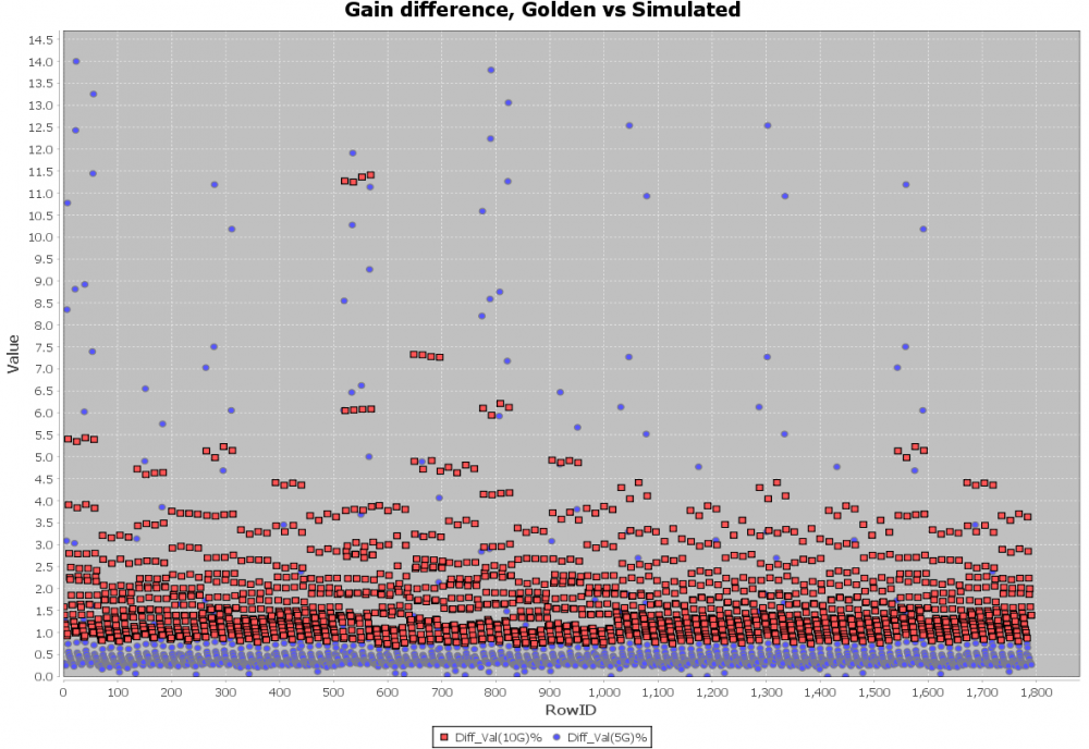
A scattering plot like below will quickly indicate which AMI parameter combinations may not work properly in newly created AMI models. In this case, one needs to go back to the modeling stage to check the codes then do this sweep validation all over again.

Channel correlation:

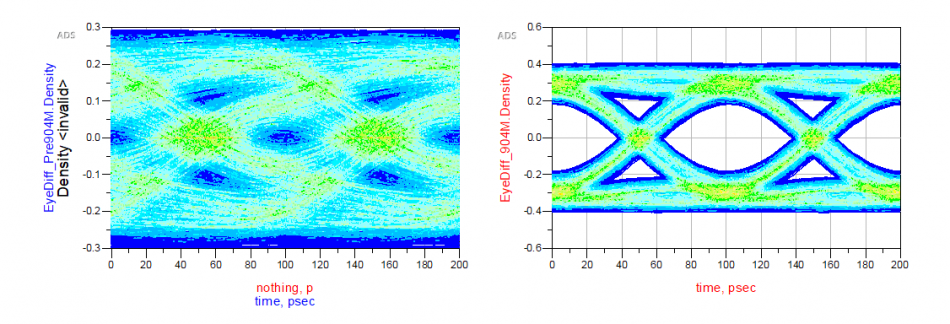
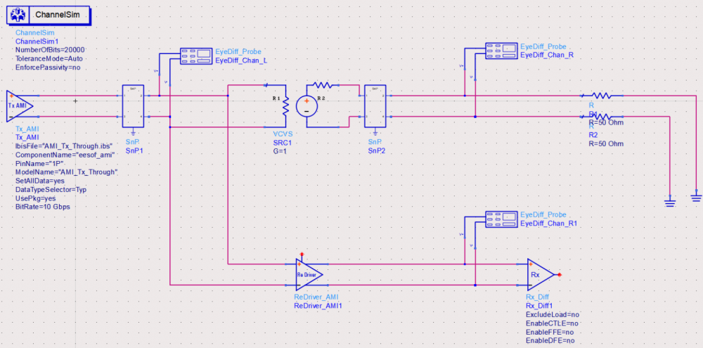
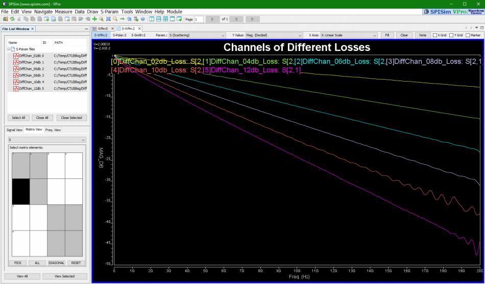
The model validation mentioned in previous section is only for a single model, not the full channel. So one still needs to pick several full channels set-up to fully qualify the models. A caveat of the channel analysis is that it only shows time domain data regardless the flow is “statistical” or “bit-by-bit”, that means it is often not easy to qualify frequency domain component such as CTLE. In this case, a corresponding s-parameter whose Sdd12 (differential input to differential output) is represented by this CTLE AMI settings can be used for an apple-to-apple comparison, like schematic shown below:

Another required step here is to test with different EDA vendor’s tool. This presents another challenge because channel simulator is usually pricey and it’s rarely the case that one company will have all of them (e.g. ADS, HyperLynx, SystemSI, QCD and HSpice etc). Different EDA tools does invoke AMI models differently… for example, some simulator passes absolute path for DLL_Path reserved parameter while others only sent relative path. So without going through this step, it’s difficult to predict what a model will behave on different tools.

Documentation:

Once all these are done, the final step is of course to create an AMI model usage guide together with some sample set-ups. Usually it will starts with IBIS model’s pin model associations and some performance chart, followed by descriptions of different AMI parameters’ meaning and mapping to the data sheet. One may also add extra info. such as alternatives if the user’s EDA tool does not support newer keyword such as Dll_Path, Dll_ID or Supporting_Files etc. Waveform comparison between original data (silicon measurement vs AMI results) should also be included. Finally it will be beneficial to provide instructions on how an example channel using this model can be set-up in popular EDA tools such as ADS, HyperLynx or HSpice.

Summary:

There you have it.. the end-to-end AMI modeling process without touching programming details! Both AMI API and programming languages are moving targets as they both evolve with time. Thus one must continue honing skills and techniques involved to be able to deliver good quality models efficiently and quickly. This is a task which requires disciplines and experience of different domains. After sharing these with you readers, do you still want to do it yourself? 🙂 Happy modeling!

A quick and easy IBIS modeling flow

For engineers who are new to IBIS modeling, the “IBIS CookBook” [LINK HERE] is a very good reference document to get started. The latest version, V4.0, was created back in 2005. While most of the documented extraction procedures still hold true to this date, some of them may be tedious or even ambiguous in terms of executions. This is particular true for processes mentioned in Chapter 4, differential buffer modeling. Further more, most recent IBIS summit presentations focus on “new and hot” topics like IBIS-AMI modeling methodologies and not many are for the traditional IBIS. In this post, I would like to first review these “formal” process, dive into how each modeling table is extracted and used in simulation, then propose a “quick and easy” method particular for differential buffer. I will then summarize with and this approach’s pros and cons.

IBIS model components:

The most basic IBIS building block, as defined in Spec. Version 3.2, is shown above. Typically at least six tables will be included in an output type buffer. They are IV (Pull-up, Pull-down) and Vt( Rising and falling) under two different test load conditions. Additional clamp IV table (Power and Ground clamp) may be added for input type buffer. After Spec version V5.1, Six additional IT tables for ISSO_PU/PD/Composite currents have also been added to address PDN effects. To create an IBIS model, the data extraction processes start with exciting particular portion of the buffer so that measured data can be post-processed to formulate as a spec-compatible table format. Because a model also has TYP/MIN/MAX skews, so the number of simulations are basically the aforementioned number of tables times three. That is, for a most basic IBIS modeling, one may need to simulate at least eighteen cases (or simulation  “decks”).

To explain a little bit more regarding blocks untouched by proposed new method, I list them in the bullets below:

  • Package/Pin parasitics: IBIS cookbook and normal modeling flow do not mention about this part. Usually a buffer package’s model is extracted using tools such as HFSS or Q3d into a form of S-parameters or equivalent broad-band spice model. An IBIS model can use a lumped R+L+C structure to describe pin specific or package (apply to all pins) specific parasitics. Alternatively, an IBIS model can also use a more detailed tree structure package model shown below for non-lumped structure. Regardless, it’s HFSS or Q3D’s task to convert such extracted S-parameter or multi-terminal sub-circuit into these simple lumped RLC values or tree structures to be included in an IBIS file. It’s a separated process and not discussed here as a part of the buffer modeling.

  • C_Comp: At the very beginning, there is only a C_Comp value between pad and ground and it is used to describe frequency dependent behavior besides the parasitics. Later on, tool like HSpice introduces extra simulation syntax to split this single C_Comp value into branches between pad and various power terminals for better accuracy. Even later, this type of syntax was adopted as part of the IBIS spec. Still, user may only find how a single C_Comp value is computed in most materials. Briefly speaking, they can be calculated using time-domain method based on RC charging/discharging time constant or freq-domain method based on the imaginary current at a particular frequency. How to split this single value into several ones to match the frequency plot best remains an art (i.e. not standardize). In addition, the value C_Comp is not visible during modeling… their effects are only shown when there are reflections back from the other end due to impedance mismatch. What we have found is that usually an IC designer has a better idea about how this value should be and the aforementioned time/frequency domain calculation method may not produce an accurate estimate.

  • Clamp current: Power/Ground clamp currents and Pull-up/Pull-down currents are both IV based (i.e. dc steady state). So they are combined for load-line analysis during simulation. The difference between Pull-up/Pull-down and Clamp is that the latter one (i.e. Clamp) can’t be turned-off. So its effect is always there even when we are extracting IV for Pull-up/Pull-down structures. Thus to avoid “double-counting”, the post-processing stage needs to remove the clamp current from pull-up/pull-down currents first before putting them into separated table. To simplify the situation… particular for an output differential buffer, we may just use IV data even though this is an IO buffer.
  • IT current: These are different dc or transient based sweep in order to obtain buffer’s drawing current when power or ground are not “ideal”. This is important in DDR case when the DQ is single ended and it’s subjective to PDN’s noise. For differential application like SERDES, PDN’s effects are usually present at both the P and N terminals and will cancel with each other. Thus their extraction may be skipped for a differential buffer mostly. One may also note that the IT extraction of composite current is “synchronized” with VT extraction of rising/falling waveform so these current data are extracted with additional “probes” rather than separated simulation.

Full IBIS modeling flow:

The process suggested in IBIS’s cookbook can be summarized as the following steps. They are also implemented in our “Full IBIS modeling flow” within SPIBPro:

  • 0, Collect design data and collateral: A modeler needs to gather PVT (process, voltage, temperature) data, silicon design, buffer terminals’ definitions and bias conditions etc. A buffer may have several tuning “legs” and bit-set settings so a modeler needs to determine which will be used for TYP, MIN and MAX corners.
  • 1, Prepare working space: Create a working space on the disk.
  • 2, Generate simulation inputs: Generate simulation “decks” to excite different block of the buffer…one at a time. So one will have eighteen or more decks at the end of this stage waiting to be simulated.
  • 3, Perform simulations: Perform simulation either sequentially on a local machine or with a simulation “farm”. Double check the results and make sure they make sense, otherwise, go back to step 0 to see which settings may be incorrect or missing.
  • 4, Generate IBIS model: Post-process the simulation data and generate IBIS model. This is usually done by the tool like ours as manual process is tedious and error prone.
  • 5, Syntax check: First quality check of an IBIS model is that it must pass the golden checker. The check here is mostly syntax-wise though there are also basic behavior check such as monotonicity or DC mismatch etc.
  • 6, Validate IBIS model: A formal validation for an IBIS model is to hook-up test load and make sure they produce correlated results comparing to those from silicon at the end of step 3 above.
  • 7, Performance report: The modeler needs to extract the performance such as PU/PD impedance values and slew rate etc. for documentation purpose and check against the spec. or data sheet.

Full step-by-step modeling flow in SPIBPro

Data extraction for a single-ended buffer:

For a single-ended buffer, the first hurdle in the modeling process is to make sure each blocks are excited properly and simulation results make sense. As mentioned, there are at least eighteen simulation needs to be done:

There are also some complications regarding the DC simulation part: some of the buffer may have “clocking” and it’s not easy to separate them from the buffer iteself. Also,  there may be many RC parasitics between nodes for a buffer netlist extracted from post-layout. In other cases one can’t even separate the actual IO part from the pre-driving portions and the resulting circuits to be simulated become huge and time consuming. These situations will make IV data extraction slow and often problematic. As a result, a simple step 0~7 modeling process may not work properly and one need to iterate to tune the set-up such that simulation will always converge and resulting IV curve be monotonic. Nevertheless, the single buffer’s modeling is easier to manage.

Data extraction for a differential buffer:

Differential buffer’s IBIS modeling extends the challenge and effort to another dimension…literally! First of all, each pin in an IBIS file or component connect to an IBIS model and the possible structures and connections between different pins are very limited. So for a differential buffer, a series element needs to be created to describe the coupling relations between pins. All the pictures used in this paragraph are from IBIS cookbook and user may find further descriptions there.

In order to construct such series model, the IV sweep needs to be performed in two dimensions, both at similar resolutions. So if say a typical single-ended IV curve has one hundred points, then the second dimension should also have that much data. That means for one particular corner, there will be one hundred IV simulation in order to construct the 2D response surface shown below. First stage post-processing also needs to be preformed so that common-mode current can be eliminated. All these need to be done before formulating a 2D data view. Only after one can visualize the resulting data, he or she can determine what components are needed to create such series model. This presents the first challenges on top of the IV simulation issues mentioned for single-ended buffer.

The second challenge is regarding the VT simulation. The current flow through this newly constructed series element needs to be “eliminated” to avoid being double counted. For spice-like simulator, there is no such thing as “negative resistance”, “negative capacitance” etc. So one has to resort to approaches like control elements or even Verilog-A (as we presented in IBIS Summit 2016) to have proper VT data extracted. For control-source based approach, it is only limited describe pin couplings of a simple R/C but not non-linear resistance or surface such as series mosfet. For that, an intermediate step to map device or equation parameters to the calculated 2d surface is needed. Even using Verilog-A’s look-up table, the grid resolution is limited by the step size used in first two-dimensional IV step and may have non-convergence issue if it’s to coarse. That’s why in the cook book (the first two lines in the picture below), it doesn’t suggest any approach as it’s really not that easy!

Due to these two great challenges, we have found that differential modeling may not be easy for most modeler. We feel more this way when providing modeling service to clients who wants to perform simulations themselves then send us data. They may want to do so due to IP concern or they knowing more about the design. In those cases, the back-and-forth tuning and tweaking process become a burden on their side and also delay the whole schedule. Thus we are motivated to find an alternative “quick-and-easy” approach to substitute the “formal” modeling steps mentioned above. While being able to simulate accurately w/ great performance is still number one priority, we are ok that they can only be used under some context (such as channel simulation).

Quick and easy approach:

In previous post, we explained how IBIS model’s data are used in a circuit simulation. Simply speaking, the “VT” data is considered as “target” while “IV” tables are used to compute so called “switching coefficients” so that appropriate amount of current will be injected or withdrawn from the buffer pad to achieve. When this is true, the nodal voltage specified by that VT table at that particular time point will be satisfied due to KCL/KVL. Now there are switching coefficients for both pull-up and pull-down structures… thus it takes two equations to solve these two unknowns. That’s why two set of VT, each under different test loads, are required. Based on this algorithm, an IV data and calculated coefficients are actually “coupled” and affect each other. If current in IV table is larger, than the calculated coefficients will become smaller and vice versa. This way the overall injected/withdrawn current will still meet KCL/KVL required for VT. In this sense, the actual IV data is not that important as it will always be “adjusted” or “weighted” by the parameters.

On the other hand, the VT data also contains several DC points and they need to be correlate to the IV table, otherwise DC mismatch errors will be thrown by the golden checker. In addition, the IV data is limited to 100 points and they need to be monotonic to avoid convergence issue. So if we have several sets of VT data and one under normal test load (say 100 ohms for a differential buffer), then they will give us “hints” regarding how IV data will look like.

With this assumption, we propose the following quick-N-easy modeling steps:

  • Connect the silicon buffer to nominal loading conditions and obtain VT simulation data
    • For Single-ended, these are simple VT waveform under two different test loads;
    • For Differential, say use nominal 100 ohms first and see voltage range between V1 and V2
      • Let V3 = (V1 + V2) / 2, use VFixture = V3 and RFixture = say 40 & 60 respectively to obtain two waveforms;
      • Alternatively, use RFixture = 50 and VFixture = say (V1 + V3) / 2, (V2 + V3) / 2 respectively to obtain two waveforms;
      • The main goals is to have two set or set-up covering operating range when a nominal test load (say 100 ohms) is used.
  • Obtain C_Comp values from buffer IC designer
  • Obtain voltage range, temperature etc parameters.

And that’s all, through carefully implemented algorithm and computation, we can generate an IBIS model based on these data with minimal simulation requirements. An the generated model is guaranteed to be error/warning free.

While we will not disclose how these are actually done in details, we can show how they are incorporated in our SPIBPro… as shown below. As a matter of fact, this process has been used in the modeling projects of past year and shown great success.

Only two VT simulation data are required to create an IBIS model

Pros and cons:

We use this approach to create differential IBIS for channel analysis purpose (together with AMI) and have not yet found any problems. Having that said, I would offer several pros and cons for reader’s considerations:

Pros:

  • Minimal simulation required and easy to perform;
  • Will be mathematically correct: no DC mismatch or monotonic warnings, output will match provided VT waveform under nominal test load.

Cons:

  • May not be accurate if the model is used for DC sweep as the IV data in the model are artificially generated;
  • No “disable” or High-Z state as clamp currents (if there are any) has been incorporate into IV data without separation;
  • No Power-aware consideration as ISSO_PU/ISSO_PD generation are not taken into account.

Summary:

In this blog post, we reviewed the formal IBIS modeling process described in the cook book, challenges modelers will face and proposed an alternative “quick-and-easy” approach to address these issues. The proposed flow uses minimum simulation data while maintaining great accuracy. There might be limitations on models generated this way such as neither disable state nor power-aware data are accounted. However, in the context of channel analysis particular when a differential model is used together with its IBIS-AMI model, we have found great success with this flow. We have also incorporated this algorithm to our SPIBPro so our tool users can benefit from this efficient yet effective flow.

IBIS-AMI: Something about CTLE

Overview:

Continuous time linear equalizer, or CTLE for short, is a commonly used in modern communication channel. In a system where lossy channels are present, a CTLE can often recover signal quality for receiver or down stream continuous signaling. There have been many articles online discussing how a CTLE works theoretically. More thorough technical details are certainly also available in college/graduate level communication/IC design text book. In this blog post, I would like to focus more on its IBIS-AMI modeling aspect from a practical point of view. While not all secret sauce will be revealed here:-), hopefully the points mentioned here will give reader a good staring point in implementing or determining their CTLE/AMI modeling methodologies.

[Credit:] Some of the pictures used in this post are from Professor Sam Palermo’s course webpage linked below. He was also my colleague at Intel previously. (not knowing each other though..)

ECEN 720: High-Speed Links Circuits and Systems


What and why CTLE:

The picture above shows two common SERDES channel setups. While the one at the top has a direct connection between Tx and Rx, the bottom one has a “repeater” to cascade up stream and down stream channels together. This “cascading” can be repeated more than once so there maybe more than two channels involved. CTLE may sit inside the Rx of both set-ups or the middle “ReDriver” in the bottom one. In either case, the S-parameter block represents a generalized channel. It may contain passive elements such as package, transmission lines, vias or connectors etc. A characteristic of such channel is that it presents different losses across spectrum, i.e. dispersion.

For example, if we plot these channel’s differential input to differential output, we may see their frequency domain (FD) loss as shown above.

Digital signals being transmitted are more or less like sequence of bit/square pulse. We know that very rich frequency components are generated during its sharp rising/falling transition edges. Ideally, a communication channel to propagate these signals should behave like an (unit-gain) all pass filter. That is, various frequency components of the signal should not be treated equally, otherwise distortion will occur. Such ideal response can be indicated as the green box below:

In reality, such all pass filter does come often. In order to compensate our lossy channels (as indicated by the red box) to be more like the ideal case (green box) as an end result, we need to apply equalization (indicated by blue box). This is why an equalizer is often used… basically it provides a transfer function/frequency response to compensate the lossy channel in order to recover the signal quality. A point worth taken here is that the blue box and red box are “tie” together. So using same equalizer for channels of different losses may cause under or over compensated. That is, an equalizer is related to the channel being compensated. Another point is that CTLE is just a subset of such linear equalizer.

CTLE is a subset of linear equalizer:

A linear equalizer can be implemented in many different ways. For example, a feed-forward equalizer is often used in the Tx side and within DFE:

FFE’s behavior is more or less easier to predict and its AMI implementation is also quite straight forward. For example, a single pre-tap or post-tap’s FFE response can be easily visualized and predicted:

Now, a CTLE is a more “generalized” linear equalizer, so its behavior is usually represented in terms of frequency responses. Thus, to accommodate/compensate channels of different losses, we will have different FD responses for CTLE:

Now that IBIS-AMI modeling for CTLE is of concern, how do we obtain such modeling data for CTLE and how they should be modeled?

Different types of CTLE modeling data:

While CTLE’s behavior can be easily understood in frequency domain, for IBIS-AMI or channel analysis, it eventually needs to come back to time domain (FD) to convolve with inputs. This is because both statistical or bit-by-bit mode of link analysis are in time domain. Thus we have several choice: provide model FD data and have it converted to TD inside the implemented AMI model, or simply provide TD response directly to the model. The benefit of the first approach is that model can perform iFFT based on analysis’ bit rate and sampling rate’s settings. The advantage of the latter one is that the provided TD model can be checked to have good quality and model does not need to do similar iFFT every time simulation starts. Of course, the best implementation, i.e. like us SPISim’s approach, is to support both modes for best flexibility and expandability 🙂

  • Frequency domain data:

Depending on the availability of original EQ design, there are several possibilities for FD data: Synthesized with poles and zeros, extract from S-parameters or AC simulation to extract response.

  1. Poles and Zeros: Given different number of poles, zeros and their locations along with dc boost level, one can synthesize FD response curves:So say if we are given a data sheet which has EQ level of some key frequencies like below: Then one can sweep different number and locations of poles and zeros to obtain matching curves to meet the spec.:
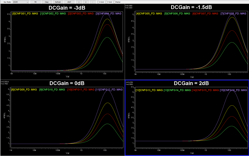
Such synthesized curves are well behaved in terms of passivity and causality etc,  and can be extended to covered desired frequency bandwidth.
  2. Extract from S-parameters: Another way to obtain frequency response is from EQ circuit’s existing S-parameter. This will provide best correlation scenarios for generated AMI model because the raw data can serve as a design target. However, there are many intermediate steps one have to perform first. For example, the given s-parameter may be single ended and only with limited frequency range (due to limitation of VNA being used), so if tool like our SPISim’s SPro is used, then one needs to: reording port (from Even-Odd ordering, i.e. 1-3, 2-4 etc to Sequential ordering, i.e. 1, 2 -> 3, 4), then convert to differential/mixed mode, after that extrapolate toward dc and high frequencies (many algorithms can be used and such extrapolation must also abide by physics) and finally extract the only related differential input -> differential output portion data.
  3. AC simulation: This assumes original design is available for AC simulation. Such raw data still needs to be sanity checked in terms of loss and phase change. For example, if gain are not flat toward DC and high-frequency range, then extra fixing may be needed otherwise iFFT results will be spurious.
  • Time domain data: time domain response can be obtained from aforementioned FD data by doing iFFT directly as shown below. It may also be obtained by simulating original EQ circuit in time domain. However, there are still several considerations:
  1. How to do iFFT: padding with zeros or conjugate are usually needed for real data iFFT. If the original FD data is not “clean” in terms of causality, passivity or asymptotic behavior, then they need to be fixed first.
  2. TD simulation: Is simulating impulse response possible? If not, maybe a step response should be performed instead. Then what is the time step or ramp speed to excite input stimuli? Note that during IBIS-AMI’s link analysis, the time step being used there may be different from the one being used here, so how will you scale the data accordingly. Once a step response is available, successive differentiation will produce impulse response with proper scaling.

How to implement CTLE AMI model:

Now that we have data to model, how will they be implemented in C/C++ codes to support AMI API for link analysis is another level of consideration.

  • Decision mechanism: As mentioned previously, a CTLE FD response targets at a channel of certain loss, thus the decision to use appropriate CTLE settings based on that particular channel at hand must either be decided by user or the model itself. While the former (user decision) does not need further explanation, the latter case (model decision, i.e. being adaptive) is a whole different topic and often vendor specific.

Typically, such adaptive mechanism has a pre-sorted CTLE in terms of strength or EQ level, then a figure-of-merit (FOM) needs to be extracted from equalized signal. That is, apply a tentative CTLE to the received data, then calculate such FOM. Then increase or decrease the EQ level by using adjacent CTLE curves and see whether FOM improves. Continue doing so until either selected CTLE “ID” settles or reach the range bounds. This process may be performed across many different cycles until it “stabilized” or being “locked”. Thus, the model may need to go through training period first to determine best CTLE being used during subsequent link analysis.

  • EQ configurations:

So now you have a bunch of settings or data like below, how should you architecture the model properly such that it can be extended in the future with revised CTLE response or allow user to perform corner selections (which essentially adds another dimension):

This is now more in software architecture domain and needs some trade-off considerations. For example, you may want to provide fine grid full spectrum FD/TD response but the data will may become to big. So internal re-sampling may be needed. For FD data, the model may needs to sample to have 2^N points for efficient iFFT. Different corner/parameter selection should not be hard coded in the models because future revised model’s parameter may be different. For external source data, encryption is usually needed to protect the modeling IP. With proper planning, one may reuse same CLTE module in many different design without customization on a case-by-case basis.

  • Correlations:

Finally it’s time to correlate the create CTLE AMI model against original EQ design or its behavioral model. Done properly, you should see signals being “recovered” from left to right below:

However, getting results like this in the first try may be a wishful thinking. In particular, the IBIS-AMI model does not work alone… it needs to work together with associated IBIS model (analog front-end) in most link simulator. So that IBIS model’s parasitics and loading etc will all affect the result. Besides, the high-impedance assumption of the AMI model also means proper termination matching is needed before one can drop them in for direct replacement of existing EQ circuit or behavioral models for correlation.

Summary:

At this point, you may realize that while a CTLE can be easily understood from its theoretic behavior perspective, its implementation to meet IBIS-AMI demands is a different story. We have seen CTLE models made by other vendor not expandable at all such that the client need to scratch the existing ones for minor revised CTLE behavior/settings (also because this particular model maker charges too much, of course). It’s our hope that the learning experience mentioned in this post will provide some guidance or considerations regardless when you decide to deep dive developing your own CTLE IBIS-AMI model, or maybe just delegate such tasks to professional model makers like us 🙂

IBIS Model: Model parameters and Spec.

Given one or more IBIS models, if all of them passed golden parser and meet my speed requirements, how do we know which one will be best fit for my channel? In this post, we are going to propose several IBIS performance parameters. It’s out hope that with these parameters, we can easily make comparison between different IBIS models and will pick the best candidate for our high speed design need.

IbisRttROn


The basic IBIS data structure is shown above, which we should have been familiar with by now. There is both pull-up (PU) and pull-down (PD) circuits which will decide the steady state output impedance. There are ESD circuits represented by power clamp (PC) and ground clamp (GC) which operates in reverse bias condition normally. How fast the PU turns from OFF to ON state and PD from ON to OFF state determines how the transient rising response of this buffer is, similar for the falling state. Due to the reverse bias condition of PC/GC, the leakage current is usually very small.

RttTerm

Another situation is like the figure above. In this case, there are on-die termination associated with buffer. Thus the current when buffer is in high-Z state will be significant…much larger than the leakage current of PC and GC.

From these two common usage scenarios, it seems reasonable that we can use both output impedance and timing response, represented by rise/fall time and slew rate as bases for our IBIS model performance parameters.

IBIS output impedance:

If the buffer’s output impedance does not match immediate connected output, usually the break out region of package represented by transmission lines. There will be significant reflection and cause damage the signal quality from the very beginning. The usual remedy is to add a series resistor such that the total output impedance will match 50 ohms, the usual characteristics impedance of a transmission line. The figure below show a typical ringing caused by impedance mismatch.

ZMismatch

Note that the PU and PD may have different impedance value around reference voltage, say 50% of Vcc, thus one common choice of series resistor to be added is the average of PU/PD impedance around that region.

IBIS timing parameters:

For better signal integrity, it is usually desired to have just fast enough signal with smooth transition edge, rather than fast signal like square wave. We have all seen the following decomposition of a square wave, as shown below. Starting with pure sin wave with same fundamental frequency, the more harmonics are added together, the more the resulting waveform will look like a square wave.

Harmonics

Signals of different frequencies will have different traveling speed along the propagation medium, thus cause the signal distortion. This phenomena has a special term called “dispersion”. So the slower the rising edge, meaning the closer it appears like fundamental sin wave, the less dispersion there will be. And thus our propagated signal will suffer less distortion.

Spec. Parameters:

With the simple discussions above, we propose the following parameters as a measure of a qualified IBIS model:

  • PVT: i.e. corner, voltage and temperature. These are information given already in an IBIS model. One needs to make sure first that the operation range is within these spec. to have desired performance presented in the IBIS model.
  • C_Comp: information given in the IBIS model for lumped capacitance at pad.
  • Z_PU: impedance of PU circuit at the reference voltage;
  • Z_PD: impedance of PD circuit at the reference voltage;
  • Z_PU_MM in %: impedance mismatch of PU circuit at some tolerance above and below the reference voltage. It’s like linearity measurement between VOH and VOL for PU circuit.
  • Z_PD_MM in %: impedance mismatch of PD circuit at some tolerance above and below the reference voltage. It’s like linearity measurement between VOH and VOL for PD circuit.
  • Z_RTT: This is the impedance representing aforementioned termination resistor(s);
  • RT: time duration between 20%~80% of voltage swing during rising transition;
  • FT: time duration between 20%~80% of voltage swing during falling transition;
  • FREQ: maximum operable frequency without buffer being overclocked.

Note that some people may use Tco, the propagation delay between buffer output and its digital input, as  parameters as well. It’s our believe that these Tco parameters are not too meaningful. We mentioned in earlier posts that a modeling engineer or circuit simulator may sacrifice the leading steady state portion of the VT curve in order to capture most portion of the transition behavior in high speed design. Tco is not kept in the model in these case. Also, SI engineers often look at the quality with eye plot, which is folded signal of different bits. There is no eye impact (eye height or eye width) by the Tco parameters as the full response to the input bit sequence has been shifted with the same amount of time, difference of true Tco and model presented Tco value.

With these parameters, one may generate a summarized table when given a library of IBIS models and will be able to find the best candidate for driving signal down the communication channel.


Generate spec. model:

Using these spec. parameters, we may further define and generate IBIS model for our early stage signal study. We can do the sweep on some of these parameters and generate artificial IBIS model accordingly. With this model for simulation and the analysis results, an SI engineer may provide this as a feedback to the circuit designer for desired performance. As a modern buffer is usually controlled by many “legs”, a circuit design should be able to find certain combinations of these “ON” lags to satisfy the system engineer’s need, or use the feedback as a guideline in fine tuning their buffer control circuit.

SPISim BPro's Spec. model generation

SPISim BPro’s Spec. model generation

With this concept, SPISim BPro takes one step further to support spec model generation, as shown in screenshot above. User can enter the appropriate settings and the corresponding IBIS model, with rising and falling waveform table included, will be generated instantaneously without any simulation. One then may use the manual waveform editor as needed to fine tune the transition waveform shape based on this spec. model.

BPro generated spec model will have smooth transitions.

BPro generated spec model will have smooth transitions.


IBIS model: How does IBIS work

* Buffer model: What is in an IBIS model:

IBISType

IBIS Spec defines many different buffer model types, as shown above. Different model types requires different modeling data to be included in the IBIS model section. In general, an IBIS model will have the following info.

  • Operational conditions: such as voltage and temperature range for operations
  • Parasitics/Loading conditions: such as C_Comp of the model. This value does not impact buffer performance when output is well terminated.
  • I/V table: These are I vs V tables of different corners for pull-up (PU), pull-down (PD), power clamp (PC) and ground clmap (GC) circuitry. They are general representations of non-linear resistor like those E elements used in the hspice circuit. According to the spec, the sweep range for these table should be from -Vcc to 2Vcc where Vcc is the power supply voltage. The reason is that in case of total reflection from the far side of the loss-less channel, either to do fully open or fully connected to ground, added full Vcc voltage swing will extend the original 0 ~ Vcc range to -Vcc to 2Vcc. Also notice that for IV sweep of pull-up circuitry, i.e. PU and PC, the voltage is Vcc relative. That means value of I when V = 0 is actually when V = 0 to Vcc = Vcc to ground. One usually needs to make such conversion back to be VSS relative during debugging process. SPISim’s IBIS module, SPIBPro, has such a GUI button to translate Vcc relative to Vss relative waveform directly.
    IBISPUPD
    IBISPCGC
  • ISSO PU/PD: These are current tables introduced in V5.0, used when terminal VCC and VSS voltages are not ideal. With lower VCC voltage due to PDN network (i.e. voltage droop), buffer strength will become weaker. So are those caused by ground bounce. This phenomena is usually called “Gate modulation effect”. ISSO/PU and PD data defines the effective current of the pull-up/pull-down structures as a function of the voltage on the pull-up/pull-down reference nodes (ideal is Vcc and Vss/Gnd)
  • V/T table: These are tables representing buffer’s voltage at die output vs elapsed buffer switching time. Under different loading condition, such as test load and test fixture, resulting waveform will be different. An ibis model usually will include at least two such VT tables under different loading condition to provide sufficient coverage during real world operations.
    IBISVT
  • I/T table: These are tables representing buffer’s drawing current vs elapsed buffer switching time. It needs to be synchronized with aforementioned VT table so that current drawn happens at the exactly same time point for the same test fixture. This current is usually composed of bypass current, pre-driver current crow-bar current and termination current if present.
    IBISIT

* How is IBIS modeling data used during circuit simulation:
With so many tables, one may wonder how they are used in a circuit simulator. To simplify, let’s first remove the ESD protection circuitry PC and GC as they are usually reversed biased and contribute very small amount of current. For the remain PU and PD circuitry, we can imagine them as non-linear resistors, similar to those MOSFET’s channel resistance when terminal voltages varies. How these two table work together during different loading condition decide the resulting transient VT waveform shown in the VT/IT table.
IBISKuKd0

During rising transition, PU circuitry gradually turns to fully ON while PD circuit gradually turns to fully OFF. Similarly, during falling transition, PU gradually turns to fully OFF and PD turns ON. Thus we can define a time dependent parameter, “switching coefficient”, which will be applied to PU and PD separately such that the resulting current from these two branches mimic the gradually turning ON/OFF effect.
IBISKuKd1

Let’s call these two switching parameters Ku(t) and Kd(t). We needs two equations to solve these two unknowns. Now assuming we have to such VT table under different loading condition. At each time point of these two tables, we know the loading condition and instant output voltage of the buffer. Using these, we can solve Ku(t) and Kd(t) in which the time, t, is buffer switched elapsed time. That is, the x-axis of the VT table.

If we don’t have two waveform table, one may make an assumption that Ku(t) + Kd(t) = 1 at all times. This is usually true at the static high or static low output condition but may not be in between. One may also use ramp parameters in the IBIS model to generate an artificial VT table for the same purpose.
IBISKuKd2

For an IBIS model developer for circuit simulator, he/she needs to consider all the branch current to obtain accurate Ku(t), Kd(t) solutions. So reverse bias current from ESD circuit need to be put in and so is the current flowing through C_Comp. For example, i=C_Comp * dV/dt can be sued to subtract current flow through this capacitor from the total output current and avoid double counting.

IBISCComp

For power-aware model, another level of scaling parameter needs to be applied. These new parameter need to scale the buffer output strength based on the instant nodal voltages across buffer terminals such that gate modulation effect will be taken into account.

Interested reader may find detailed algorithm in the following two paper.

IBIS model: What is IBIS

IBIS is short of I/O Buffer Information Specification. The spec. was proposed in early 90’s to promote tool independent I/O models for system level analysis. It’s been evolved since even until this date. It’s now an ANSI standard and are widely supported by different system level EDA vendors, including SPISim.

IBISLogo
IBIS model is created as a behavoiral model for transistor’s buffer deisgn used in system level analysis. Several milestones and its delta improvements have been listed briefly below:

  • Version 3.2, using IV/VT data table to address and meet most signal integrity’s needs.
  • Version 4.0, introduces other language such as Verilog-A, VHDL and Berkeley spice as external circuits to address shortcomings of rigid IBIS syntax, which often is not flexible enough to represent behaviors more advanced buffer design.
  • Version 5.0 introduces power aware features. By introducing ISSO PU/PD and Composite Current which represents currents drawn from power delivery network (PDN), the voltage droop and ground bounce issues during simultaneous switching can be modeled and analyzed.
  • Version 5.1 introduce AMI to account for equalization mechanism which sits transmitter’s analog front end and behind receiver’s buffer output. AMI model is mostly written in C/C++ compiled into .Dll or .so loaded by simulator. This deviation from more high level language such as Verilog-A gave model designers tremendous flexibility in modeling the full EQ + buffer to enable bit-error-rate based analysis. However, it also significantly increase the barriers and difficulties to create a good buffer model.

IBISEvolve

When talking about the term “IBIS””, one needs to distinguish about IBIS Spec, an IBIS file and a IBIS model. The following list gives simple overview:

  • IBIS Spec: Spec. defined by IBIS committee. In addition to the buffer related portion, its general meanings may also include connector spec (ICM, InterConnect modeling Spec). ICM provides standard model format for all electrical interconnects such as cables, connectors, package and printed PCB. Previously, a different spec, EBD… electric board description was used. ICM is to replace EBD.
  • IBIS File: An IBIS file is like a container of models for an IC or chipset. An IC package usually has many pins, with several buffers inside. Thus an IBIS file usually have manufacturer’s info as part of the headers, followed by different pins, pin names and connected buffers, then detailed various buffer models and their modeling data. An IBIS file may also have package models and AMI statements which points to associated .ami and .dll/.so files for corresponding equalizer portion of the design.
  • IBIS Model: An IBIS model is an individual buffer model sits inside the IBIS file. Depending on modeling type and the IBIS version, it may have I/T, V/T, I/V data tables and corresponding operation and loading condition when these model are being excited for modeling. It’s desired the usage of this buffer model should not deviate from the modeling condition too much as the behavior in those range may not cover properly in the constructed model.
IBIS Files vs Models

IBIS Files vs Models

Viewing model data of an IBIS file in SPIBPro

Viewing model data of an IBIS file in SPIBPro