* Buffer model: What is in an IBIS model:
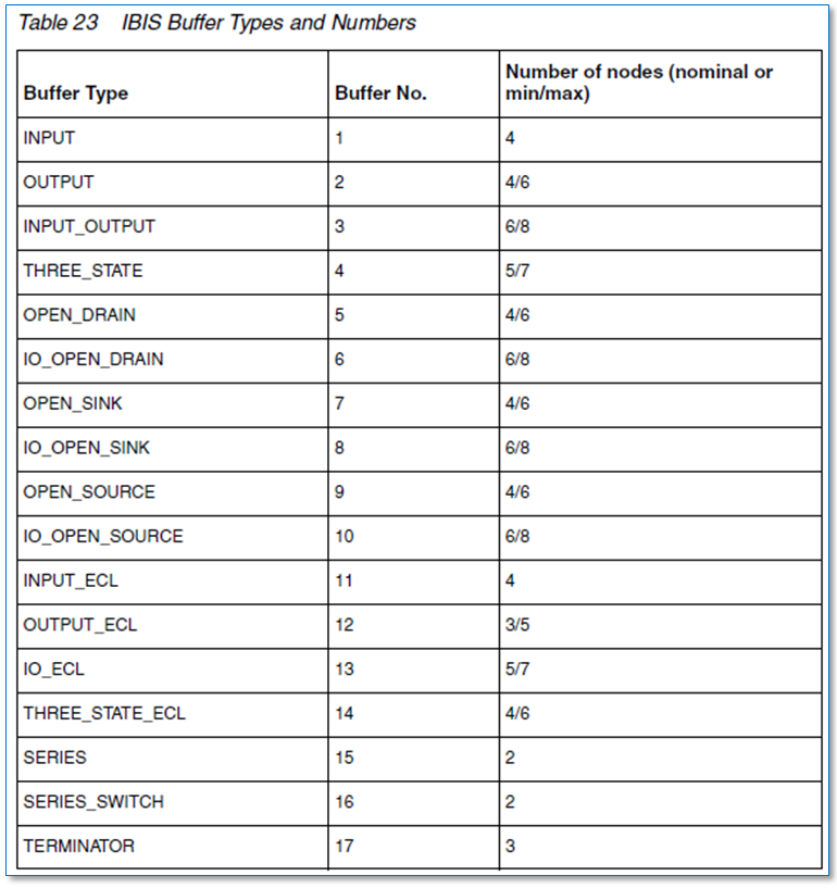
IBIS Spec defines many different buffer model types, as shown above. Different model types requires different modeling data to be included in the IBIS model section. In general, an IBIS model will have the following info.
- Operational conditions: such as voltage and temperature range for operations
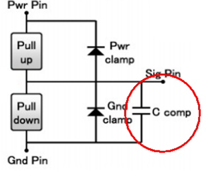
- Parasitics/Loading conditions: such as C_Comp of the model. This value does not impact buffer performance when output is well terminated.
- I/V table: These are I vs V tables of different corners for pull-up (PU), pull-down (PD), power clamp (PC) and ground clmap (GC) circuitry. They are general representations of non-linear resistor like those E elements used in the hspice circuit. According to the spec, the sweep range for these table should be from -Vcc to 2Vcc where Vcc is the power supply voltage. The reason is that in case of total reflection from the far side of the loss-less channel, either to do fully open or fully connected to ground, added full Vcc voltage swing will extend the original 0 ~ Vcc range to -Vcc to 2Vcc. Also notice that for IV sweep of pull-up circuitry, i.e. PU and PC, the voltage is Vcc relative. That means value of I when V = 0 is actually when V = 0 to Vcc = Vcc to ground. One usually needs to make such conversion back to be VSS relative during debugging process. SPISim’s IBIS module, SPIBPro, has such a GUI button to translate Vcc relative to Vss relative waveform directly.
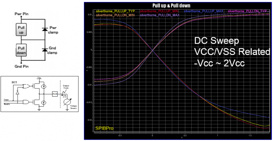
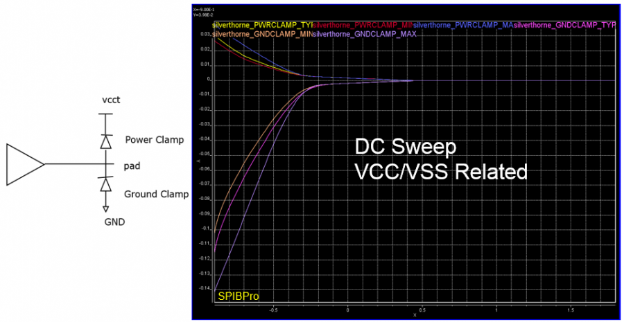
- ISSO PU/PD: These are current tables introduced in V5.0, used when terminal VCC and VSS voltages are not ideal. With lower VCC voltage due to PDN network (i.e. voltage droop), buffer strength will become weaker. So are those caused by ground bounce. This phenomena is usually called “Gate modulation effect”. ISSO/PU and PD data defines the effective current of the pull-up/pull-down structures as a function of the voltage on the pull-up/pull-down reference nodes (ideal is Vcc and Vss/Gnd)
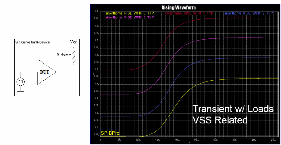
- V/T table: These are tables representing buffer’s voltage at die output vs elapsed buffer switching time. Under different loading condition, such as test load and test fixture, resulting waveform will be different. An ibis model usually will include at least two such VT tables under different loading condition to provide sufficient coverage during real world operations.
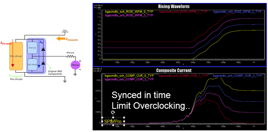
- I/T table: These are tables representing buffer’s drawing current vs elapsed buffer switching time. It needs to be synchronized with aforementioned VT table so that current drawn happens at the exactly same time point for the same test fixture. This current is usually composed of bypass current, pre-driver current crow-bar current and termination current if present.
* How is IBIS modeling data used during circuit simulation:
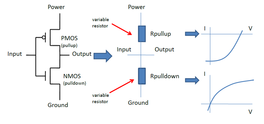
With so many tables, one may wonder how they are used in a circuit simulator. To simplify, let’s first remove the ESD protection circuitry PC and GC as they are usually reversed biased and contribute very small amount of current. For the remain PU and PD circuitry, we can imagine them as non-linear resistors, similar to those MOSFET’s channel resistance when terminal voltages varies. How these two table work together during different loading condition decide the resulting transient VT waveform shown in the VT/IT table.
During rising transition, PU circuitry gradually turns to fully ON while PD circuit gradually turns to fully OFF. Similarly, during falling transition, PU gradually turns to fully OFF and PD turns ON. Thus we can define a time dependent parameter, “switching coefficient”, which will be applied to PU and PD separately such that the resulting current from these two branches mimic the gradually turning ON/OFF effect.
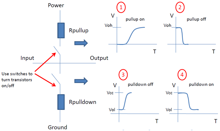
Let’s call these two switching parameters Ku(t) and Kd(t). We needs two equations to solve these two unknowns. Now assuming we have to such VT table under different loading condition. At each time point of these two tables, we know the loading condition and instant output voltage of the buffer. Using these, we can solve Ku(t) and Kd(t) in which the time, t, is buffer switched elapsed time. That is, the x-axis of the VT table.
If we don’t have two waveform table, one may make an assumption that Ku(t) + Kd(t) = 1 at all times. This is usually true at the static high or static low output condition but may not be in between. One may also use ramp parameters in the IBIS model to generate an artificial VT table for the same purpose.
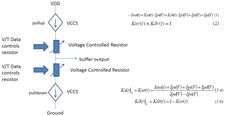
For an IBIS model developer for circuit simulator, he/she needs to consider all the branch current to obtain accurate Ku(t), Kd(t) solutions. So reverse bias current from ESD circuit need to be put in and so is the current flowing through C_Comp. For example, i=C_Comp * dV/dt can be sued to subtract current flow through this capacitor from the total output current and avoid double counting.
For power-aware model, another level of scaling parameter needs to be applied. These new parameter need to scale the buffer output strength based on the instant nodal voltages across buffer terminals such that gate modulation effect will be taken into account.
Interested reader may find detailed algorithm in the following two paper.
- The Development of Analog SPICE Behavioral Model Based on IBIS Model, by Ying Wang, Han Ngee Tan
- Extraction of Transient Behavioral MOdel of Digital I/O BUffers from IBIS, by Peivand, F. Tehrani, Yuzhe Chen, Jiayuan Fang


Pingback: A quick an easy IBIS modeling flow | SPISim: EDA for Signal Integrity, Power Integrity and Circuit Simulation
This page provides very good explaination about how to use IBIS.
I have a question about V-T. How should this ramp rate be used for calculate the output I?
After switching low to high or high to low, the elapsed time since switching can be used to extrapolate the voltage. Current can be calculated or interpolated from the I-V table.
This page shares good information about the IBIS model.
I am trying for the first time to develop an IBIS model. So, I have lots of doubts.
How to start developing the IBIS model?
What should be the steps to be followed to get a Power aware IBIS model?
Why do we need a power clamp, ground clamp diodes, and C_comp?
To start IBIS modeling, checkout the cookbook on ibis.org.
Power and ground clamps are for ESD projection. C_Comp represents parasitic capacitance.