A quick and easy IBIS modeling flow

For engineers who are new to IBIS modeling, the “IBIS CookBook” [LINK HERE] is a very good reference document to get started. The latest version, V4.0, was created back in 2005. While most of the documented extraction procedures still hold true to this date, some of them may be tedious or even ambiguous in terms of executions. This is particular true for processes mentioned in Chapter 4, differential buffer modeling. Further more, most recent IBIS summit presentations focus on “new and hot” topics like IBIS-AMI modeling methodologies and not many are for the traditional IBIS. In this post, I would like to first review these “formal” process, dive into how each modeling table is extracted and used in simulation, then propose a “quick and easy” method particular for differential buffer. I will then summarize with and this approach’s pros and cons.

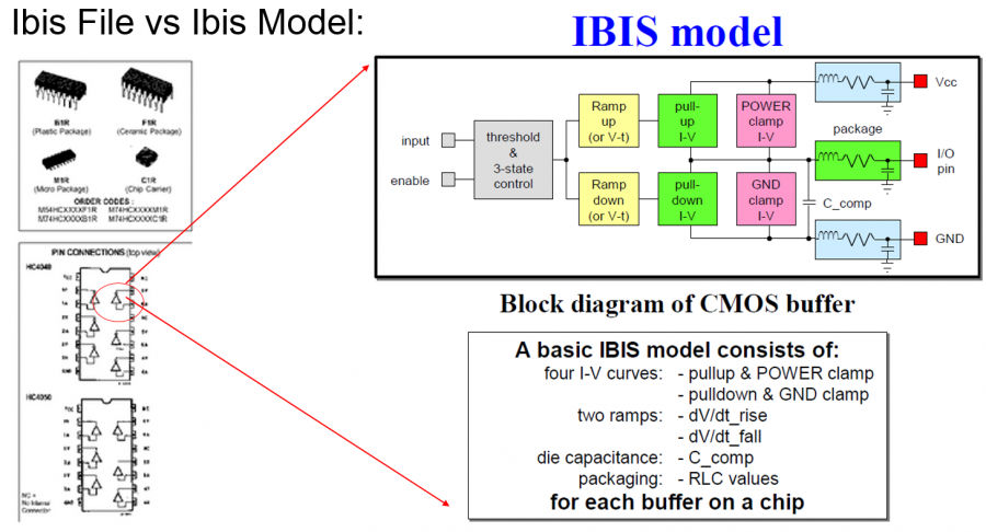
IBIS model components:

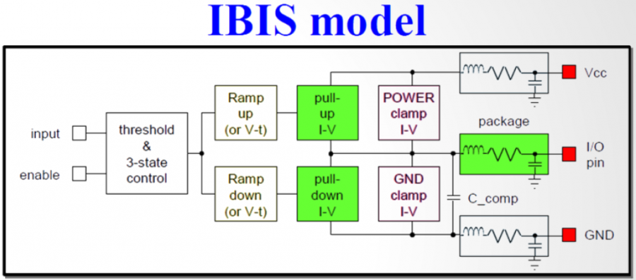
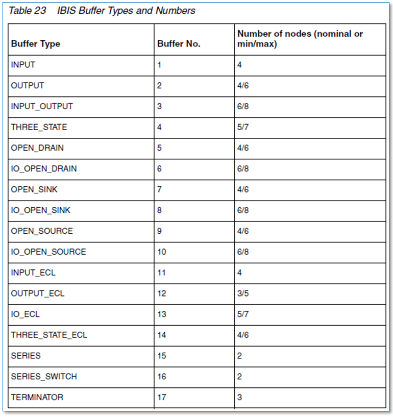
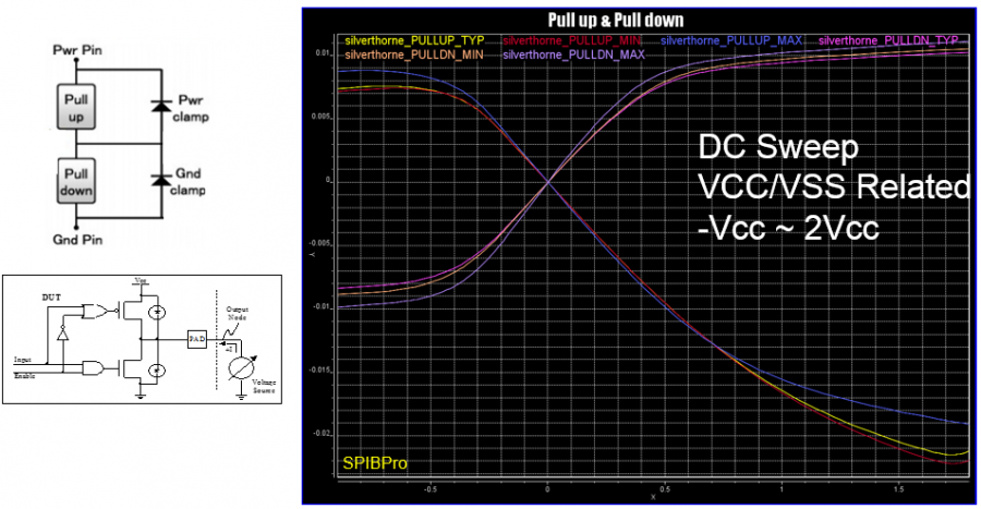
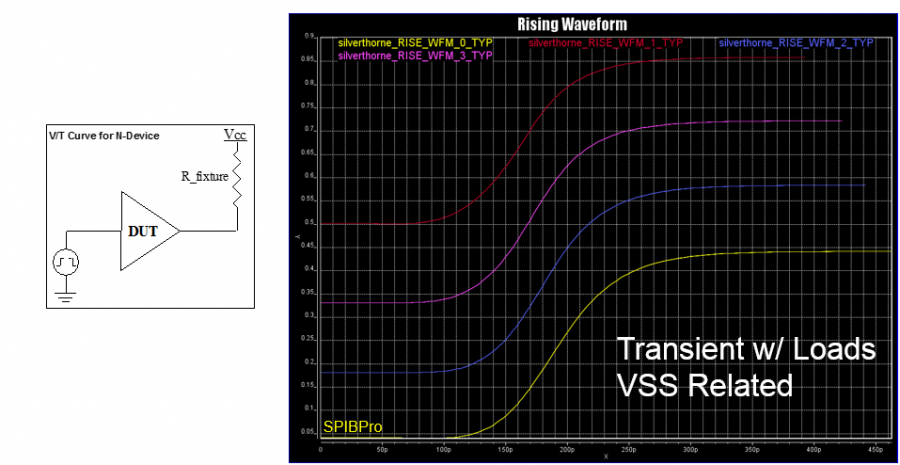
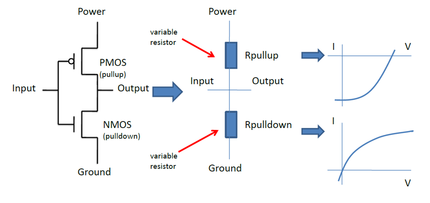
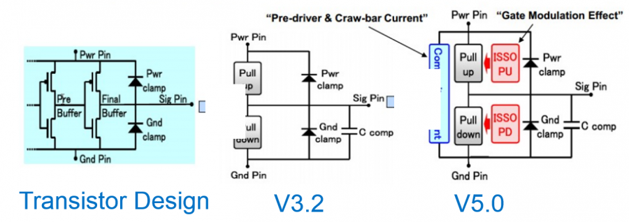
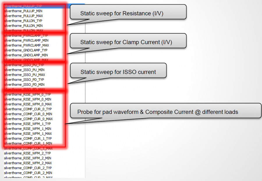
The most basic IBIS building block, as defined in Spec. Version 3.2, is shown above. Typically at least six tables will be included in an output type buffer. They are IV (Pull-up, Pull-down) and Vt( Rising and falling) under two different test load conditions. Additional clamp IV table (Power and Ground clamp) may be added for input type buffer. After Spec version V5.1, Six additional IT tables for ISSO_PU/PD/Composite currents have also been added to address PDN effects. To create an IBIS model, the data extraction processes start with exciting particular portion of the buffer so that measured data can be post-processed to formulate as a spec-compatible table format. Because a model also has TYP/MIN/MAX skews, so the number of simulations are basically the aforementioned number of tables times three. That is, for a most basic IBIS modeling, one may need to simulate at least eighteen cases (or simulation  “decks”).

To explain a little bit more regarding blocks untouched by proposed new method, I list them in the bullets below:

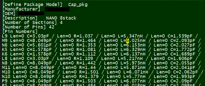
  • Package/Pin parasitics: IBIS cookbook and normal modeling flow do not mention about this part. Usually a buffer package’s model is extracted using tools such as HFSS or Q3d into a form of S-parameters or equivalent broad-band spice model. An IBIS model can use a lumped R+L+C structure to describe pin specific or package (apply to all pins) specific parasitics. Alternatively, an IBIS model can also use a more detailed tree structure package model shown below for non-lumped structure. Regardless, it’s HFSS or Q3D’s task to convert such extracted S-parameter or multi-terminal sub-circuit into these simple lumped RLC values or tree structures to be included in an IBIS file. It’s a separated process and not discussed here as a part of the buffer modeling.

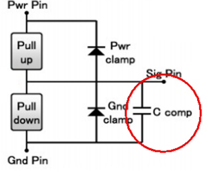
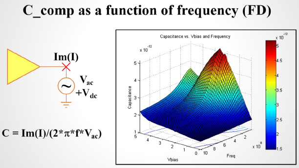
  • C_Comp: At the very beginning, there is only a C_Comp value between pad and ground and it is used to describe frequency dependent behavior besides the parasitics. Later on, tool like HSpice introduces extra simulation syntax to split this single C_Comp value into branches between pad and various power terminals for better accuracy. Even later, this type of syntax was adopted as part of the IBIS spec. Still, user may only find how a single C_Comp value is computed in most materials. Briefly speaking, they can be calculated using time-domain method based on RC charging/discharging time constant or freq-domain method based on the imaginary current at a particular frequency. How to split this single value into several ones to match the frequency plot best remains an art (i.e. not standardize). In addition, the value C_Comp is not visible during modeling… their effects are only shown when there are reflections back from the other end due to impedance mismatch. What we have found is that usually an IC designer has a better idea about how this value should be and the aforementioned time/frequency domain calculation method may not produce an accurate estimate.

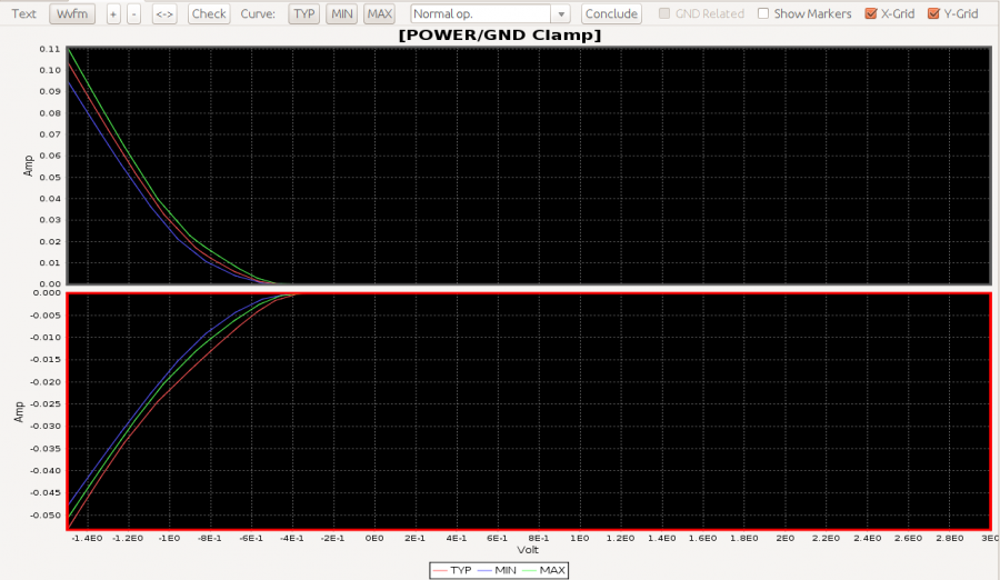
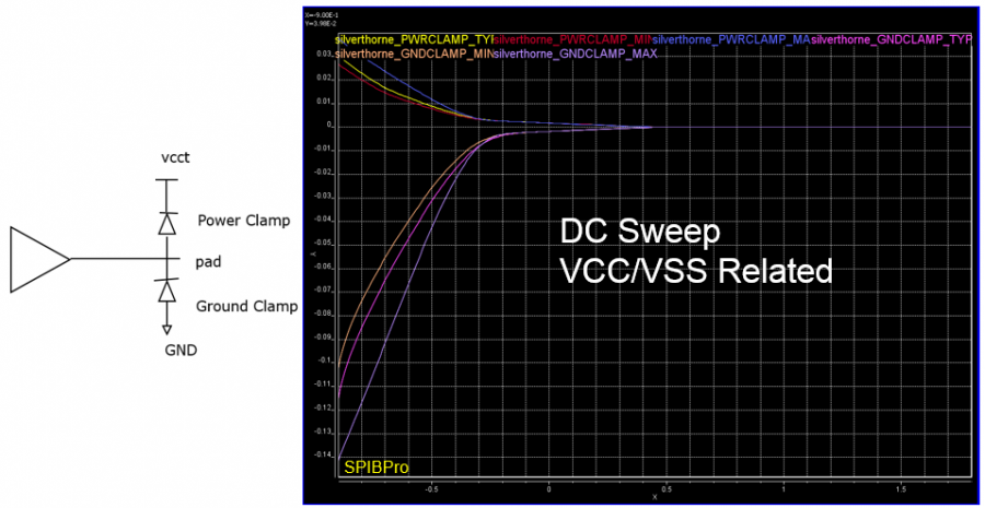
  • Clamp current: Power/Ground clamp currents and Pull-up/Pull-down currents are both IV based (i.e. dc steady state). So they are combined for load-line analysis during simulation. The difference between Pull-up/Pull-down and Clamp is that the latter one (i.e. Clamp) can’t be turned-off. So its effect is always there even when we are extracting IV for Pull-up/Pull-down structures. Thus to avoid “double-counting”, the post-processing stage needs to remove the clamp current from pull-up/pull-down currents first before putting them into separated table. To simplify the situation… particular for an output differential buffer, we may just use IV data even though this is an IO buffer.
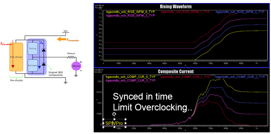
  • IT current: These are different dc or transient based sweep in order to obtain buffer’s drawing current when power or ground are not “ideal”. This is important in DDR case when the DQ is single ended and it’s subjective to PDN’s noise. For differential application like SERDES, PDN’s effects are usually present at both the P and N terminals and will cancel with each other. Thus their extraction may be skipped for a differential buffer mostly. One may also note that the IT extraction of composite current is “synchronized” with VT extraction of rising/falling waveform so these current data are extracted with additional “probes” rather than separated simulation.

Full IBIS modeling flow:

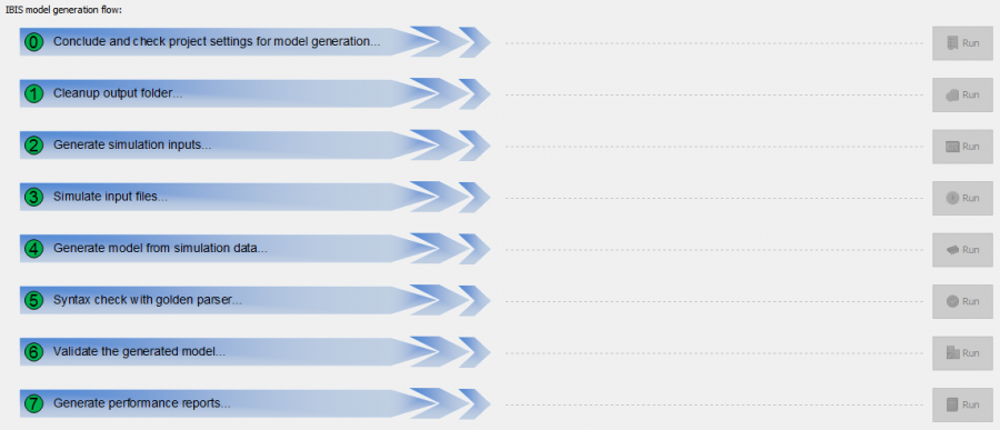
The process suggested in IBIS’s cookbook can be summarized as the following steps. They are also implemented in our “Full IBIS modeling flow” within SPIBPro:

  • 0, Collect design data and collateral: A modeler needs to gather PVT (process, voltage, temperature) data, silicon design, buffer terminals’ definitions and bias conditions etc. A buffer may have several tuning “legs” and bit-set settings so a modeler needs to determine which will be used for TYP, MIN and MAX corners.
  • 1, Prepare working space: Create a working space on the disk.
  • 2, Generate simulation inputs: Generate simulation “decks” to excite different block of the buffer…one at a time. So one will have eighteen or more decks at the end of this stage waiting to be simulated.
  • 3, Perform simulations: Perform simulation either sequentially on a local machine or with a simulation “farm”. Double check the results and make sure they make sense, otherwise, go back to step 0 to see which settings may be incorrect or missing.
  • 4, Generate IBIS model: Post-process the simulation data and generate IBIS model. This is usually done by the tool like ours as manual process is tedious and error prone.
  • 5, Syntax check: First quality check of an IBIS model is that it must pass the golden checker. The check here is mostly syntax-wise though there are also basic behavior check such as monotonicity or DC mismatch etc.
  • 6, Validate IBIS model: A formal validation for an IBIS model is to hook-up test load and make sure they produce correlated results comparing to those from silicon at the end of step 3 above.
  • 7, Performance report: The modeler needs to extract the performance such as PU/PD impedance values and slew rate etc. for documentation purpose and check against the spec. or data sheet.

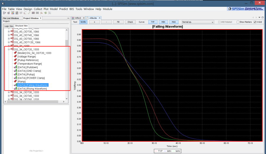
Full step-by-step modeling flow in SPIBPro

Data extraction for a single-ended buffer:

For a single-ended buffer, the first hurdle in the modeling process is to make sure each blocks are excited properly and simulation results make sense. As mentioned, there are at least eighteen simulation needs to be done:

There are also some complications regarding the DC simulation part: some of the buffer may have “clocking” and it’s not easy to separate them from the buffer iteself. Also,  there may be many RC parasitics between nodes for a buffer netlist extracted from post-layout. In other cases one can’t even separate the actual IO part from the pre-driving portions and the resulting circuits to be simulated become huge and time consuming. These situations will make IV data extraction slow and often problematic. As a result, a simple step 0~7 modeling process may not work properly and one need to iterate to tune the set-up such that simulation will always converge and resulting IV curve be monotonic. Nevertheless, the single buffer’s modeling is easier to manage.

Data extraction for a differential buffer:

Differential buffer’s IBIS modeling extends the challenge and effort to another dimension…literally! First of all, each pin in an IBIS file or component connect to an IBIS model and the possible structures and connections between different pins are very limited. So for a differential buffer, a series element needs to be created to describe the coupling relations between pins. All the pictures used in this paragraph are from IBIS cookbook and user may find further descriptions there.

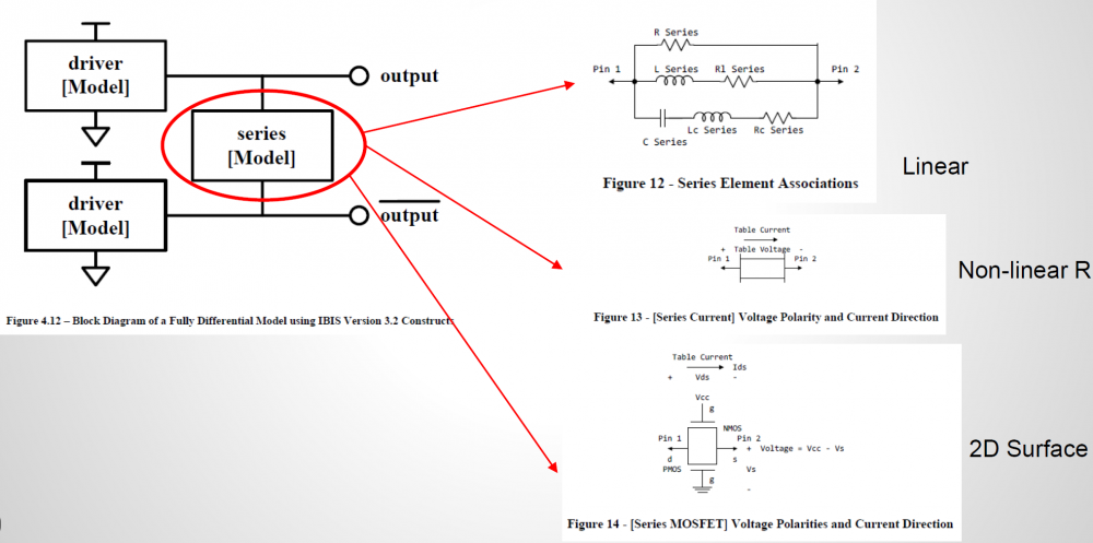
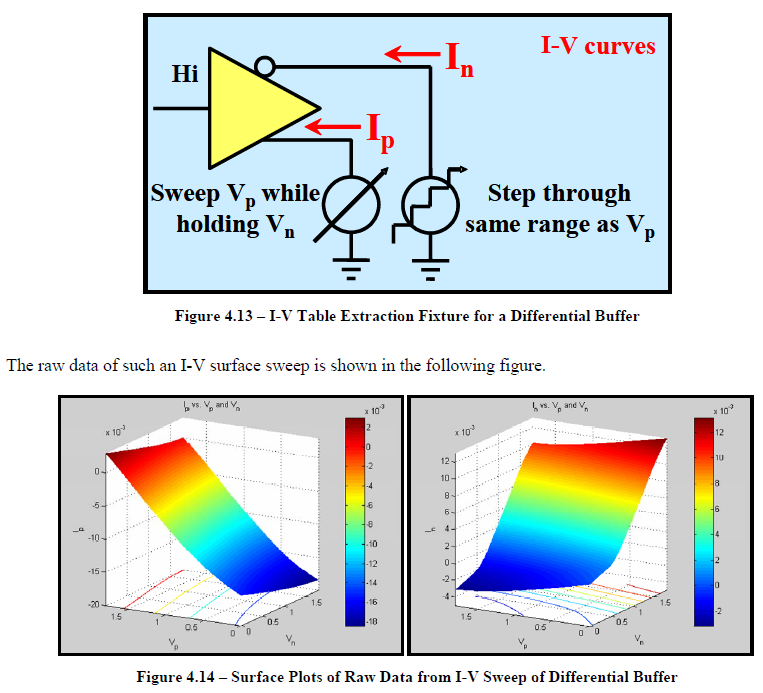
In order to construct such series model, the IV sweep needs to be performed in two dimensions, both at similar resolutions. So if say a typical single-ended IV curve has one hundred points, then the second dimension should also have that much data. That means for one particular corner, there will be one hundred IV simulation in order to construct the 2D response surface shown below. First stage post-processing also needs to be preformed so that common-mode current can be eliminated. All these need to be done before formulating a 2D data view. Only after one can visualize the resulting data, he or she can determine what components are needed to create such series model. This presents the first challenges on top of the IV simulation issues mentioned for single-ended buffer.

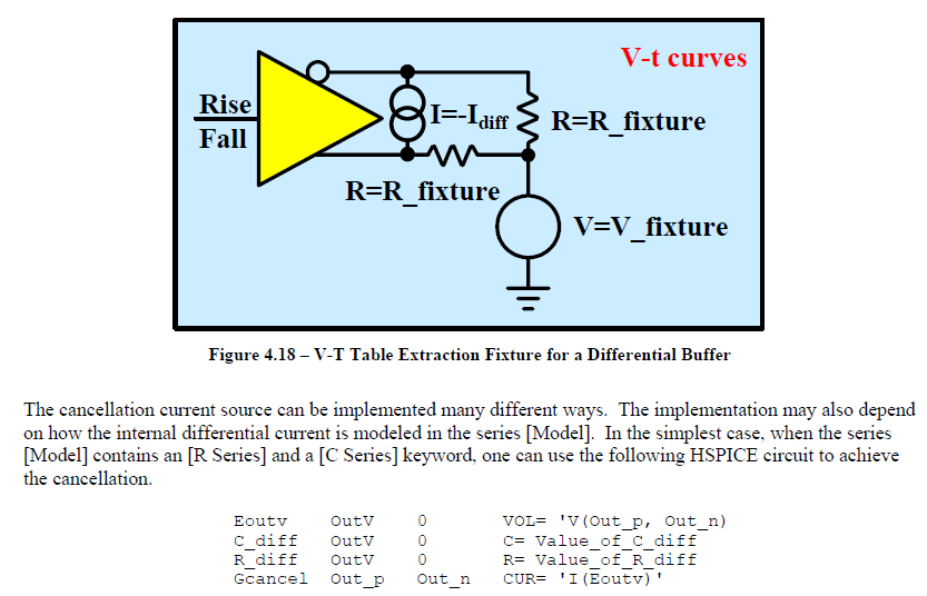
The second challenge is regarding the VT simulation. The current flow through this newly constructed series element needs to be “eliminated” to avoid being double counted. For spice-like simulator, there is no such thing as “negative resistance”, “negative capacitance” etc. So one has to resort to approaches like control elements or even Verilog-A (as we presented in IBIS Summit 2016) to have proper VT data extracted. For control-source based approach, it is only limited describe pin couplings of a simple R/C but not non-linear resistance or surface such as series mosfet. For that, an intermediate step to map device or equation parameters to the calculated 2d surface is needed. Even using Verilog-A’s look-up table, the grid resolution is limited by the step size used in first two-dimensional IV step and may have non-convergence issue if it’s to coarse. That’s why in the cook book (the first two lines in the picture below), it doesn’t suggest any approach as it’s really not that easy!

Due to these two great challenges, we have found that differential modeling may not be easy for most modeler. We feel more this way when providing modeling service to clients who wants to perform simulations themselves then send us data. They may want to do so due to IP concern or they knowing more about the design. In those cases, the back-and-forth tuning and tweaking process become a burden on their side and also delay the whole schedule. Thus we are motivated to find an alternative “quick-and-easy” approach to substitute the “formal” modeling steps mentioned above. While being able to simulate accurately w/ great performance is still number one priority, we are ok that they can only be used under some context (such as channel simulation).

Quick and easy approach:

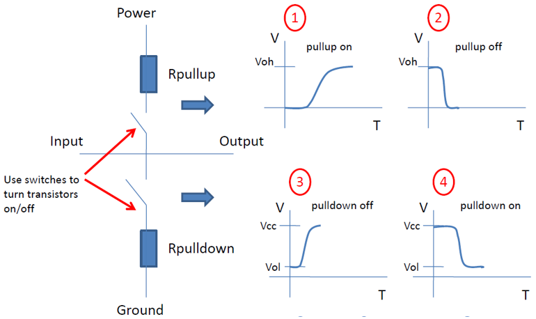
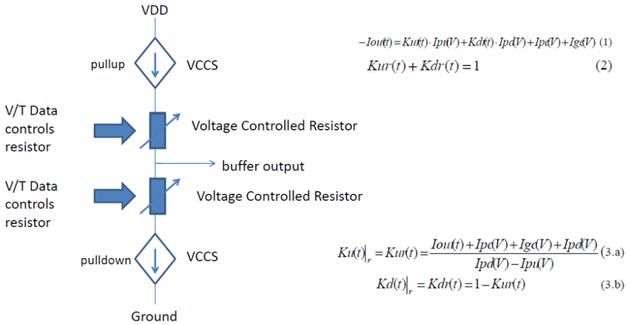
In previous post, we explained how IBIS model’s data are used in a circuit simulation. Simply speaking, the “VT” data is considered as “target” while “IV” tables are used to compute so called “switching coefficients” so that appropriate amount of current will be injected or withdrawn from the buffer pad to achieve. When this is true, the nodal voltage specified by that VT table at that particular time point will be satisfied due to KCL/KVL. Now there are switching coefficients for both pull-up and pull-down structures… thus it takes two equations to solve these two unknowns. That’s why two set of VT, each under different test loads, are required. Based on this algorithm, an IV data and calculated coefficients are actually “coupled” and affect each other. If current in IV table is larger, than the calculated coefficients will become smaller and vice versa. This way the overall injected/withdrawn current will still meet KCL/KVL required for VT. In this sense, the actual IV data is not that important as it will always be “adjusted” or “weighted” by the parameters.

On the other hand, the VT data also contains several DC points and they need to be correlate to the IV table, otherwise DC mismatch errors will be thrown by the golden checker. In addition, the IV data is limited to 100 points and they need to be monotonic to avoid convergence issue. So if we have several sets of VT data and one under normal test load (say 100 ohms for a differential buffer), then they will give us “hints” regarding how IV data will look like.

With this assumption, we propose the following quick-N-easy modeling steps:

  • Connect the silicon buffer to nominal loading conditions and obtain VT simulation data
    • For Single-ended, these are simple VT waveform under two different test loads;
    • For Differential, say use nominal 100 ohms first and see voltage range between V1 and V2
      • Let V3 = (V1 + V2) / 2, use VFixture = V3 and RFixture = say 40 & 60 respectively to obtain two waveforms;
      • Alternatively, use RFixture = 50 and VFixture = say (V1 + V3) / 2, (V2 + V3) / 2 respectively to obtain two waveforms;
      • The main goals is to have two set or set-up covering operating range when a nominal test load (say 100 ohms) is used.
  • Obtain C_Comp values from buffer IC designer
  • Obtain voltage range, temperature etc parameters.

And that’s all, through carefully implemented algorithm and computation, we can generate an IBIS model based on these data with minimal simulation requirements. An the generated model is guaranteed to be error/warning free.

While we will not disclose how these are actually done in details, we can show how they are incorporated in our SPIBPro… as shown below. As a matter of fact, this process has been used in the modeling projects of past year and shown great success.

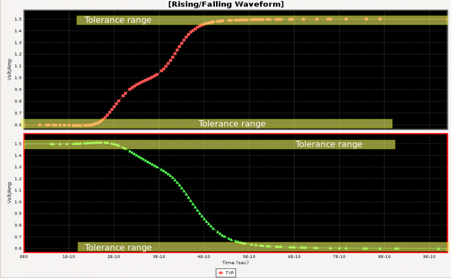
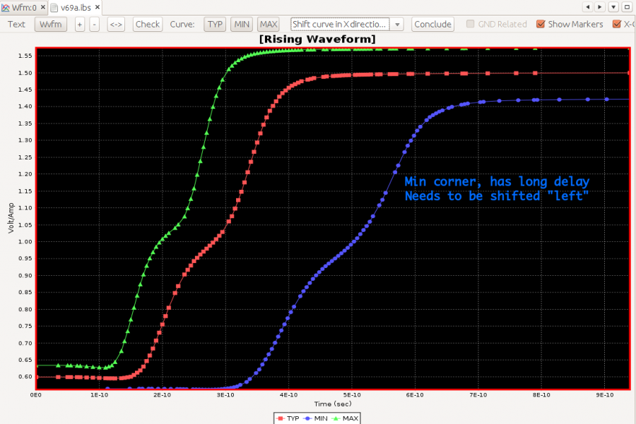
Only two VT simulation data are required to create an IBIS model

Pros and cons:

We use this approach to create differential IBIS for channel analysis purpose (together with AMI) and have not yet found any problems. Having that said, I would offer several pros and cons for reader’s considerations:

Pros:

  • Minimal simulation required and easy to perform;
  • Will be mathematically correct: no DC mismatch or monotonic warnings, output will match provided VT waveform under nominal test load.

Cons:

  • May not be accurate if the model is used for DC sweep as the IV data in the model are artificially generated;
  • No “disable” or High-Z state as clamp currents (if there are any) has been incorporate into IV data without separation;
  • No Power-aware consideration as ISSO_PU/ISSO_PD generation are not taken into account.

Summary:

In this blog post, we reviewed the formal IBIS modeling process described in the cook book, challenges modelers will face and proposed an alternative “quick-and-easy” approach to address these issues. The proposed flow uses minimum simulation data while maintaining great accuracy. There might be limitations on models generated this way such as neither disable state nor power-aware data are accounted. However, in the context of channel analysis particular when a differential model is used together with its IBIS-AMI model, we have found great success with this flow. We have also incorporated this algorithm to our SPIBPro so our tool users can benefit from this efficient yet effective flow.

IBIS model: Debug and performance tuning

In this post, we would like to talk about debugging IBIS model and performance tuning. As discussed in previous posts, one of the first and important steps to make sure IBIS model generated from simulation data is valid is to run with IBIS committee released golden parser. Often times, the parser will output the following errors or warning messages for models with suspicious qualities:

  • DC mismatch: mismatch between VT’s steady state and IV data;
  • Non-monotonic data points in I/V curve;
  • Extreme currents in IV data.

We are going to discuss these in more details below. For performance tuning, we are going to talk about buffer overclocking and the associated accuracy concerns. This is important because it will make sure your buffer will run at desired speed or lower without producing erroneous response. We also briefly talk about solution implemented in our SPIBPro modeling tool to meet the overclocking challenges.

DC mismatch:

One of the most troublesome messages output by golden parser is the DC mismatch warnings/errors:

DCMismatchMsg

When the mismatch percentage is small, what’s visible to modeling engineer is that their IBIS model will not produce exactly same dc steady state voltages comparing to those from original transistor buffer design. The usual remedy often is to go back  and check the IV simulation setup and biasing conditions then regenerate model and  check again. The last resort is to use editor like those in our BPro to manually adjust the data points mostly in IV table such that the DC mismatch will alleviate or even go away. To know how to fix this problem, we need to explain what this message means:

Steady state at the beginning and ending of the VT waveform

Steady state at the beginning and ending of the VT waveform

In the figure above, the beginning and ending points of each VT table, be it rising waveform or falling waveform, are assume to have reached steady state. These two steady states are taken by the IBIS parser to perform check for DC mismatch. During steady state, voltages are assumed to stay the same and the time point is irrelevant. Since each VT table comes with test fixture information, one may compute load line current with these two voltage points and the given fixture info.

DC mismatch is due to mismatched steady state and IV data point

DC mismatch is due to mismatched steady state and IV data point

In the figure above, we depict a buffer output to a test load setup, represented by variable R fixture to V fixture to ground in this case at the lower left. The load line current I is V / R. That is, when the nodal voltage at pad is V, the output current I can be computed as:

  • I_LoadLine = (V_Pad – V_Fixture) / R_Fixture

Now this current is contributed by those pull-up (PU, PC) and pull-down (PD, GC) circuits.  At logic high output state, we may assume PD are fully off (current contribution is 0.0), so current at this point is from PU mainly minus small reverse bias current from PC and GC. When looking at the PU’s IV table, we can find this V_Pad, minus Vcc (as PU’s voltage is “Vcc relative”), find out the I_PU for this voltage point. We can then find I_PC and I_GC similarly using PC and GC table if they are present (remember PC is also “Vcc relative”). Finally I_Out is I_PU – I_PC – I_GC. that is, based on these IV tables, this buffer will output current equivalent to I_Out. DC Mismatch means I_LoadLine is not equal to I_Out. That is, the output current computed from the VT’s ending points is not same as that computed based on the given IV tables.

What we just described is for logic high situation, i.e. ending point or rising waveform or starting point of falling waveform. For logic low output situation, the process is similar, only that in this case, PU is assumed to be fully “OFF” so most of the current drawn is from the PD branch.

Knowing the causes of this errors, then the approaches to fix become apparent. Either one may need to adjust (manually or check and re-simulate to generate) IV table, or need to check whether the VT wavform make sense or not. Our experience show that 90% of the case, IV simulation is not done correctly, either because bias condition was not setup properly, or the “pseudo-transient” methods change voltage too fast such that the current measured is not true “steady state” current.


Non-Monotonic Points in I/V data:

This messages means the table is non-monotonic, meaning the sign of its first derivative changes. Our experience shows that these types of warnings are usually OK to ignore. However, strong non-monotonicity may cause simulator trouble to find solutions around that region, thus cause non-convergence issue.

Often time these troubling points are in the non-active region of the device and can be “smooth” out easily by deleting offending or adding points. It should also be noted that some devices do exhibit non-monotonic behavior, so artificially removing them either to make it more appearing visually or to avoid parser warnings may cause concern of the model recipients about accuracy of this model, if they are also knowledgeable about this type of buffer design.


Extreme current in IV data:

ExtremeIError

This happens most common to power clamp (PC) and ground clamp (GC) data table. However, since PC/GC currents can’t be removed and must be subtracted from the PU/PD (pull-up/pull-down) current during modeling, it may also means that PC/GC currents are not captured properly in PU/PD such that after subtraction, PU/PD data table shows signs of “break down” current like those in the PC/GC.

PowerGndClamp

The picture above shown typical PC/GC curve. As one can see, most of the time (in normal buffer operating region), the curve is relative flat and value is small. This is in reverse bias region and leakage current is small. However, due to the -Vcc ~ 2Vcc requirement of the IBIS modeling to account for total reflection. the ESD circuit may well march into the “break down” region and have exponential like current output or drawn from the pad. It is in this area which may cause extreme current warning.

Since the buffer operate in ESD’s reverse bias region mostly, the approach to fix this can be simple, albeit a little artificial. One may find the data point at least 1 volt beyond points when ESD starts to breakdown and use these two points for extrapolation. This way the exponential like curves are converted to linear with still sufficient current output/drawn to allow ESD circuit, represented by PC/GC, to protect the circuits connecting to the buffer’s output.


Buffer Overclocking:

Each set of rising and falling waveform combined to form a complete period, T. The maximum frequency a circuit simulator can operate this buffer thus is FMax = 1 / T. That is, the longer the T is, the lower speed buffer can operate without letting simulator sacrificing some of model’s original data.

When a buffer is operated at a higher frequency than its models allows, FMax, this buffer is being overclocked. Overclocked buffer may produce inconsistency issue, as explained below.

Tolerance

The figure above shows a typical untrimmed VT simulation data or IBIS model VT waveform. One will find that the steady state portion occupies great portion of the data points. So if we set a tolerance range around these steady states and trim to remove those data points, we may end up with a much shorter duration of the data table which still captures the majority of the transition informatino, yet can be operated at a much higher frequency.

Normally this type of the “trimming” can be done by the circuit simulator automatically. However, being a modeling developer, you would not want to limit your user choice of simulators. Since IBIS spec does not give a clear messages how a circuit simulator should trim the data (e.g, trim from back or from the beginning, with how much tolerance?), one may often find simulation results inconsistent when different simulators are used on the same IBIS model, particular at a higher frequency.

MIN corner has much longer delay

MIN corner has much longer delay

Another example of source of overclocking is shown above. In this case, the min corner waveform, represented in blue, has much longer delay than the other two corners. Since the IBIS spec. requires that all TYP/MIN/MAX corner should share the same set of X-data (time), the MIN corner will then be easily overclocked or even won’t have enough transition information captured in the produced IBIS model.

To address this overclocking issue, SPISim propose letting user gain finer control of the trimming behavior. Also let tool take care of the tuning after trimming is done to avoid aforementioned DC mismatch issue. Another handy solution is to use editor provided by BPro to allow certain degrees of manual editing easily.

Tuning

SPISim BPro’s manual tuning capabilities

Note that besides the voltage portion we have discussed so far, power aware IBIS 5.0 model also present another challenge: The composite current, which contains crow-bar current as well, usually starts being active even when output voltage is still steady. As a result, simulator can’t trim out the leading steady state voltage because doing so, will sacrifice the current information presented in the model. We will discuss this problem and propose solution further in future post.

IBIS model: How does IBIS work

* Buffer model: What is in an IBIS model:

IBISType

IBIS Spec defines many different buffer model types, as shown above. Different model types requires different modeling data to be included in the IBIS model section. In general, an IBIS model will have the following info.

  • Operational conditions: such as voltage and temperature range for operations
  • Parasitics/Loading conditions: such as C_Comp of the model. This value does not impact buffer performance when output is well terminated.
  • I/V table: These are I vs V tables of different corners for pull-up (PU), pull-down (PD), power clamp (PC) and ground clmap (GC) circuitry. They are general representations of non-linear resistor like those E elements used in the hspice circuit. According to the spec, the sweep range for these table should be from -Vcc to 2Vcc where Vcc is the power supply voltage. The reason is that in case of total reflection from the far side of the loss-less channel, either to do fully open or fully connected to ground, added full Vcc voltage swing will extend the original 0 ~ Vcc range to -Vcc to 2Vcc. Also notice that for IV sweep of pull-up circuitry, i.e. PU and PC, the voltage is Vcc relative. That means value of I when V = 0 is actually when V = 0 to Vcc = Vcc to ground. One usually needs to make such conversion back to be VSS relative during debugging process. SPISim’s IBIS module, SPIBPro, has such a GUI button to translate Vcc relative to Vss relative waveform directly.
    IBISPUPD
    IBISPCGC
  • ISSO PU/PD: These are current tables introduced in V5.0, used when terminal VCC and VSS voltages are not ideal. With lower VCC voltage due to PDN network (i.e. voltage droop), buffer strength will become weaker. So are those caused by ground bounce. This phenomena is usually called “Gate modulation effect”. ISSO/PU and PD data defines the effective current of the pull-up/pull-down structures as a function of the voltage on the pull-up/pull-down reference nodes (ideal is Vcc and Vss/Gnd)
  • V/T table: These are tables representing buffer’s voltage at die output vs elapsed buffer switching time. Under different loading condition, such as test load and test fixture, resulting waveform will be different. An ibis model usually will include at least two such VT tables under different loading condition to provide sufficient coverage during real world operations.
    IBISVT
  • I/T table: These are tables representing buffer’s drawing current vs elapsed buffer switching time. It needs to be synchronized with aforementioned VT table so that current drawn happens at the exactly same time point for the same test fixture. This current is usually composed of bypass current, pre-driver current crow-bar current and termination current if present.
    IBISIT

* How is IBIS modeling data used during circuit simulation:
With so many tables, one may wonder how they are used in a circuit simulator. To simplify, let’s first remove the ESD protection circuitry PC and GC as they are usually reversed biased and contribute very small amount of current. For the remain PU and PD circuitry, we can imagine them as non-linear resistors, similar to those MOSFET’s channel resistance when terminal voltages varies. How these two table work together during different loading condition decide the resulting transient VT waveform shown in the VT/IT table.
IBISKuKd0

During rising transition, PU circuitry gradually turns to fully ON while PD circuit gradually turns to fully OFF. Similarly, during falling transition, PU gradually turns to fully OFF and PD turns ON. Thus we can define a time dependent parameter, “switching coefficient”, which will be applied to PU and PD separately such that the resulting current from these two branches mimic the gradually turning ON/OFF effect.
IBISKuKd1

Let’s call these two switching parameters Ku(t) and Kd(t). We needs two equations to solve these two unknowns. Now assuming we have to such VT table under different loading condition. At each time point of these two tables, we know the loading condition and instant output voltage of the buffer. Using these, we can solve Ku(t) and Kd(t) in which the time, t, is buffer switched elapsed time. That is, the x-axis of the VT table.

If we don’t have two waveform table, one may make an assumption that Ku(t) + Kd(t) = 1 at all times. This is usually true at the static high or static low output condition but may not be in between. One may also use ramp parameters in the IBIS model to generate an artificial VT table for the same purpose.
IBISKuKd2

For an IBIS model developer for circuit simulator, he/she needs to consider all the branch current to obtain accurate Ku(t), Kd(t) solutions. So reverse bias current from ESD circuit need to be put in and so is the current flowing through C_Comp. For example, i=C_Comp * dV/dt can be sued to subtract current flow through this capacitor from the total output current and avoid double counting.

IBISCComp

For power-aware model, another level of scaling parameter needs to be applied. These new parameter need to scale the buffer output strength based on the instant nodal voltages across buffer terminals such that gate modulation effect will be taken into account.

Interested reader may find detailed algorithm in the following two paper.

IBIS model: What is IBIS

IBIS is short of I/O Buffer Information Specification. The spec. was proposed in early 90’s to promote tool independent I/O models for system level analysis. It’s been evolved since even until this date. It’s now an ANSI standard and are widely supported by different system level EDA vendors, including SPISim.

IBISLogo
IBIS model is created as a behavoiral model for transistor’s buffer deisgn used in system level analysis. Several milestones and its delta improvements have been listed briefly below:

  • Version 3.2, using IV/VT data table to address and meet most signal integrity’s needs.
  • Version 4.0, introduces other language such as Verilog-A, VHDL and Berkeley spice as external circuits to address shortcomings of rigid IBIS syntax, which often is not flexible enough to represent behaviors more advanced buffer design.
  • Version 5.0 introduces power aware features. By introducing ISSO PU/PD and Composite Current which represents currents drawn from power delivery network (PDN), the voltage droop and ground bounce issues during simultaneous switching can be modeled and analyzed.
  • Version 5.1 introduce AMI to account for equalization mechanism which sits transmitter’s analog front end and behind receiver’s buffer output. AMI model is mostly written in C/C++ compiled into .Dll or .so loaded by simulator. This deviation from more high level language such as Verilog-A gave model designers tremendous flexibility in modeling the full EQ + buffer to enable bit-error-rate based analysis. However, it also significantly increase the barriers and difficulties to create a good buffer model.

IBISEvolve

When talking about the term “IBIS””, one needs to distinguish about IBIS Spec, an IBIS file and a IBIS model. The following list gives simple overview:

  • IBIS Spec: Spec. defined by IBIS committee. In addition to the buffer related portion, its general meanings may also include connector spec (ICM, InterConnect modeling Spec). ICM provides standard model format for all electrical interconnects such as cables, connectors, package and printed PCB. Previously, a different spec, EBD… electric board description was used. ICM is to replace EBD.
  • IBIS File: An IBIS file is like a container of models for an IC or chipset. An IC package usually has many pins, with several buffers inside. Thus an IBIS file usually have manufacturer’s info as part of the headers, followed by different pins, pin names and connected buffers, then detailed various buffer models and their modeling data. An IBIS file may also have package models and AMI statements which points to associated .ami and .dll/.so files for corresponding equalizer portion of the design.
  • IBIS Model: An IBIS model is an individual buffer model sits inside the IBIS file. Depending on modeling type and the IBIS version, it may have I/T, V/T, I/V data tables and corresponding operation and loading condition when these model are being excited for modeling. It’s desired the usage of this buffer model should not deviate from the modeling condition too much as the behavior in those range may not cover properly in the constructed model.
IBIS Files vs Models

IBIS Files vs Models

Viewing model data of an IBIS file in SPIBPro

Viewing model data of an IBIS file in SPIBPro