Simulator development: Modeling (S & P)

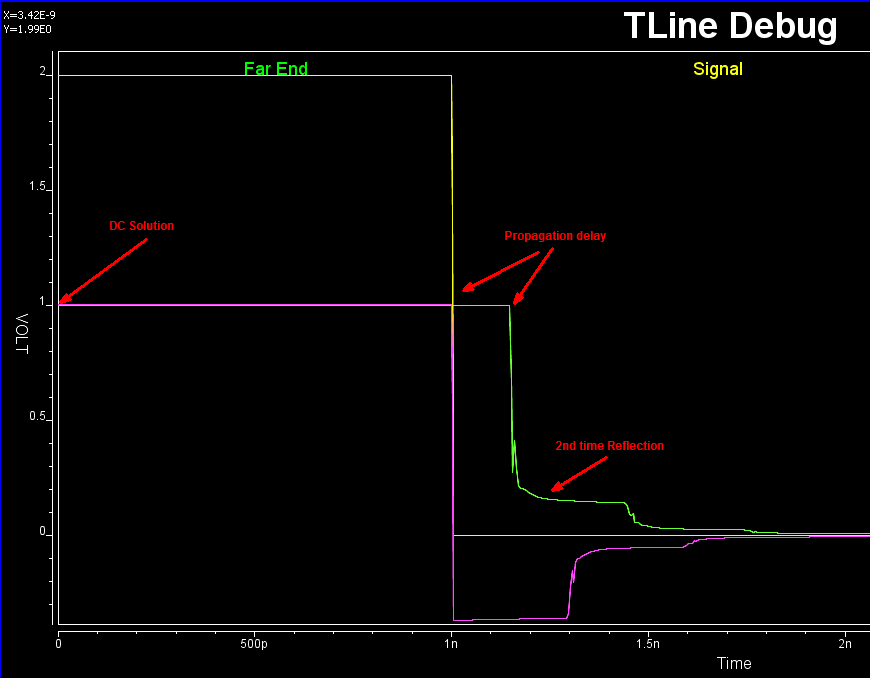
System channel is usually represented in S-parameters. They can be extracted in frequency domain using a 3D field solver, and/or cascaded stage by stage using tool like SPISim’s SPro. With LTI (linear time invariant) assumption, it’s possible to synthesize eye or BER plot of millions of bits using statistically analysis… using single time domain pulse for these parameters. However, it’s still often desired to be able to simulate the s-parameter in time domain for defined bit patterns. Thus, a system simulator like our SSolve must be able to support such requirement. In addition, one may also want to know the frequency response when given a broadband spice converted spice elements, such as via, package or connector models. So the reversed process, i.e. extract S-parameters from spice elements, is also often required. In this post, we will briefly talk about how these may be developed in simulator like SSolver.

S-Element… S-Parameters:

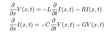
There have been many conference and journal papers proposing different methods of simulating S-parameter in time domain. However, at the most basic level, S-parameter can be considered as a transfer function or filter block. Thus DSP techniques can apply: transfer function multiplying inputs in frequency domain can be converted into time domain using convolution:

Convolusion

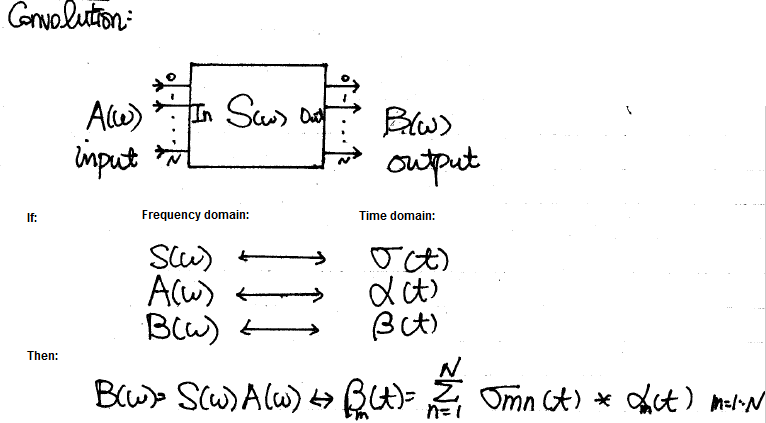
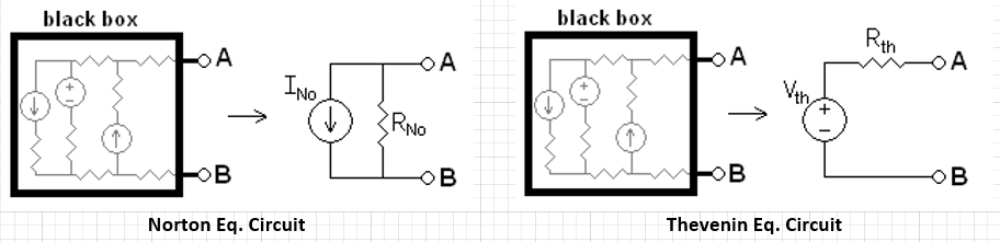
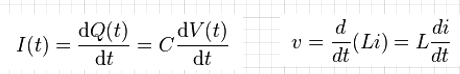
The time domain at the right hand side can be further separated into two parts: history up to this time point (integrate from -infinity to t=n-1) and the value at this particular moment t=n due to input. The first part is a constant as it’s already happened in the past and can’t be changed, the second part is, however, input dependent and must be updated within the “solve” and “stamp” hot loop inside newton iteration. When putting together, they form a Norton circuit form of I = Y * V + J where Y is value affected at this moment and J, a constant, is due to past history. This Norton form can then be “stamped” accordingly for matrix solving.

Interested reader may refer to the paper published by HP linked below for detailed explanations and math:

Integration of Transient S-Parameter Simulation into HSpice

The equation [18] and [19] is the aforementioned Norton equivalent circuit form and can be used accordingly.

The convolution method needs to update history with the solved results of this time step for next time step to be used. In addition, the basic convolution requires that the dt to be constant, thus a variable time step simulation will be greatly hampered by this requirement in terms of performance. So the convolution modeling has rooms for improvement.

One of the possible approach is using vector fitting technique mentioned in previous post about “W-element” modeling. With the S-parameter data in frequency domain, one may construct a Pade approximation using several poles and zeros. Then basis functions can be created for each of the pole in time domain and simulate accordingly. A benefit of this process is that the constructed form is a rational function which is guaranteed to be causal. So if there are issue regarding causality of the provided s-parameter, it can be fixed during the modeling process. Lastly, due to exact fitting of multi-port s-parameter across the frequency spectrum are not likely, some sort of error minimization (in the MSE sense) is needed to have a balance between accuracy and number of poles.


P-Element… Port element:

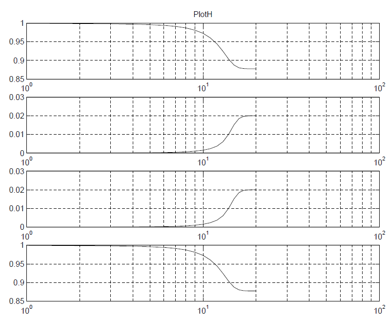
Often times after a package, connector or via modeling engineer created a model, he or she will use tool like broadband spice to convert such 3D extracted s-parameters to spice equivalent circuit composed of various basic elements. When a system designer or SI engineer receive such converted models, the original S-parameter may not be available already. Rather than insert this model into the channel and simulate blindly, it’s often beneficial to be able to reconstruct and inspect the model’s frequency domain response first before actually using them. S-Parameter extraction via simulation is basically a form of AC simulation, thus with AC model of the system elements constructed, the S-Parameter extraction part becomes easy.

The context here is small signal S-parameter extraction, thus all the AC signal is done very close to the operating point. That is, a DC solution needs to be obtained first for each port’s respecitve bias condition, then the AC stimulus is applied and solve for each frequency point.

A “Port” or “P-element” has several properties: dc bias condition, reference impedance, port-name and port-order. For a multi-port s-parameter extraction, one port is excited at a time with specified dc bias value. AC sweep is then performed while the other ports are terminated to their reference impedance. The power wave of input and output, measured and processed using current injection and nodal voltage measured, can then obtained for this input to the other output ports. Using simple math described in the link below:

S-parameter measurements

one can obtain S-parameter of Sij (i is port with input stimulus, j are the other ports) content easily this way. Repeat the same process for the other ports one at a time (with their respective dc bias condition) and the full S-parameter can be obtained. Finally, the order of ports are arranged according to the port properties, their respective port name are written out at the top of the touch stone file and the process is complete. Should there be needs to convert to other formats such as Y, Z parameter (sometimes good for checking connectivity), one can do so easily with formula (assuming generalized 2-N ports) or simply use developed tool like our SPro.


Back to the top:

Back from these modeling physics to the computer science domain, one also need to consider the following topics when doing simulator development:

  • Memory pool management (allocation, expansion and clean-up)
  • Multi-threading consideration
  • Plug-in architecture for future devices
  • ….

While the list can go on and on and the tasks may be daunting, the end results are definitely worthy to the analysis flow and methodologies development. With developed simulator, there is no longer absolute need to form a close-loop formula or equation in order to solve circuit equation. The module or flow running on top can simply create netlist and have this simulator solved for you. Not to mentioned this also make maintenance and testing much easier. For an EDA company like us, I would say this is a journey worth taking.

Simulator development: Modeling (B & W)

When modeling device for a circuit simulator, the raw netlist input needs to be converted into internal structure first, then a physical model is constructed during the “modeling” phase, and corresponding equivalent Norton or Thevenin circuits’ parameter are solved within each Newton iteration at each timestep. The solved parameters are finally “stamped”  into system matrix for Newton iteration solving. “Model” and “Solve” is the essential part of device modeling for a circuit simulator and that’s whey “Physics” come into play.

In these two posts, we will briefly talk about how system devices, in particular IBIS, Transmission line and S-parameter are “modeled” and “solved”.

B-Element… IBIS:

Looking at the IBIS’s structure, the modeling part is actually quite straight forward:

IBISEvolve

The four IV curve data: pull-up, pull-down, power clamp and ground clamp act like non-linear resistors. With terminal voltage known within each Newton iteration, the conductance can be look-up from these curve tables and obtained using linear interpolation.

The switching coefficients and composite currents are both time dependent. Their values are calculated in the “modeling” phase when simulation has not even started. The obtained coefficients is a multiplier which will further scale the conductance calculated for IV data and thus stamped value. These scaling are such that when test load specified in the waveform section is connected, driver at the pin will reproduce exactly the same waveform data given in the model. As to C-Comp, it can be inserted using simulator’s existing infrastructure so the integrator there will manage the stamping and error prediction.

The more complicated portion of IBIS modeling inside a simulator is due to the options available for the end user, thus model developer must plan in advance. For example, the c_comp may be split across different terminals. Each waveform, IV or components have different skews which book-keeping codes must take care of. There might be added submodel for pre-emphasis or de-emphasis so the class implementation-wise one should consider “composite” pattern such that recursive inclusion can happen. At the end, this is a relative simple device to model for simulator, particular when comparing to the transmission line.


W-Element… Transmission line:

Every electromagnetic text book will give transmission line structure as shown below:

RLGC

This is an uniform distributed model and is implemented early in various simulators as  the “U” element. While implements T-Line model this way is now outdated due to the performance issue, it’s still how the T-Line’s raw data, frequency dependent tabular model, are given:

TabModel

The tabular model are field solved of Maxwell’s equations based on layer stackup, trace layout, material properties and sometime special treatment (like surface roughness) and finally presented as R/L/G/C data at low (DC), high (Infinity) frequencies and many points in between. Thus to model T-Line for a simulator to use, one has to convert these data to a mathematical form first which can then be used in either time or frequency domain. For transmission line, this can starts with Telegrapher’s equations.

By solving the KCL/KVL of a unit length RLGC circuit above, one can derive and find the telegrapher’s equation:

And the solution to this equations, as explained in the wiki link above, involve a wave propagation function Gamma:

RLGCEq2

When realize this in the system model, it as the Norton equivalent circuit form:

So on each side (near end and far end) of the transmission line, there are two components: Z (admittance) at that particular time step and current source due to the propagation delay originated from the other end. These two components (Z(s) and r(s)) can be obtained from the tabular data in frequency domain and then converted to integrate-able form in time domain so that they can be “stamped”. Generally, it includes the following steps:

  • Parse and store the raw tabular model;
  • Calculate the propagation delay and characteristic impedance using highest frequency data (or using extrapolation), these value will be used for interpolation later in time domain.
  • Construct the Z(s) or Y(s) and the wave function r(s) shown in the system model. As transmission lines are usually coupled, these curves are multi-dimensional in frequency domain;
  • Using vector fitting technique to represent this frequency domain functions using series of poles and zeros. In most of the cases, particular when the model data has insufficient bandwidth or low quality, exact fit is not possible with reasonable number of poles/zeros and thus best fit in the minimum-square-error sense needs to be performed.
  • Once pole and zeros are found, they can be converted into time domain as different order of terms. All these terms combined together will form the Y(t) or r(t) in time domain. Pade’s approximation may be used here.
  • During time domain simulation, use interpolation to find r(t)’s value in the past history (propagation delay ago) and use that data to construct the equivalent model of this end at this particular time point.
  • For frequency domain analysis, vector fitting and conversion to integral form is not needed. The Y(s) and r(s) data can be used directly for stamping at this frequency with some interpolation.

For the first three steps, I wrote a simple matlab codes to demonstrate how how they are done:

Impedance function:MatlabY

Propagation function:MatlabH

Plots:PlotY

PlotH

While the matlab codes above seems straightforward,  most simulator (including SPISim’s SSolver) will program with native codes (C/C++) for performance consideration. So a whole lots of matrix operation (inverse, eigen value, LU decomposition etc) will also come into play during the process.

It’s rarely the case that the developed model or codes will work the first try. With so many terms (of converted poles and zeros) for so many dimensions (coupled cases), it’s a daunting task to figure out what has gone wrong when waveform is not as expected. It’s often simpler to back to basic: check steady state solution first, use one line, no reflection with by matching impedance at the other end, use characteristic impedance to find nominal reflection value and so on to help identifying the issue:

TLDebug

Interested reader may find more details about SPISim’s implementation, same as HSpice’s, in the following paper:

“Optimal Transient Simulation of Transmission Lines” by Dmitri Borisovich Kuznetsov, Jose E. Schutt-Aine, IEEE Trans. on Circuit and Systems, I Feb. 1996

In terms of book, I have found that Chap. 5 of Dan Oh’s “High-speed Signaling” book, S6 in our reference book section, give best explanations among others. This maybe because Mr. Oh is from UIUC around the same time when the paper was published as well 🙂 It also worth mentioning that similar technique can be applied to other passive, homogeneous device modeling, such as the system channel. For example,  one common approach of checking and fixing casual issue of a s-parameter is by using vector fitting and convert to rational function form.

Simulator development: Abstraction

In previous post regarding simulator development, we mentioned that simulator at its core is linear algebra (with or without relaxation) solving matrices formed to describe netlist’s nodal cutset (KCL) and mesh loops (KVL). We also mentioned that the “hot-loop” of circuit simulation are the “solve” and “stamp” routines, i.e., device solve modeling equations at that particular dc point or time-step then put contents into the aforementioned matrix formation. So a lot of thinking needs to go into formulating these two steps such that simulator developed is stable, maintainable and extensible.

On the p170 of the classic “Computer Methods for Circuit Analysis and Design” book, stamping for basic elements are listed:

Stamp

So the first level of abstraction, also the main work of “Solve” routine within each device, is to solve the modeling equations using terminal conditions (i.e. voltage or current) in a particular iteration, then translate into corresponding I, V, Y (admittance), G (conductance) then put into the circuit matrix for simulator to solve. In addition, because Newton method requires first derivative to progress and find next possible root, the “partial” value (first derivative of matrix) also needs to be computed by the device model and provide to the simulator accordingly. Without this, simulator will need to perform numerical derivative (auto-partial) to call “solve” and “stamp” routine multiple times in order to find the derivative dV/dI, or dI/dV etc at that particular terminal conditions. This will result slowness and instability of the circuit simulation.

Each device, regardless how non-linear it is, may be “linearized” to simple equivalent circuit under certain condition. This “certain condition” can be fixed time point, or fixed terminal condition like voltage supply. That is, within each Newton iteration (thus only belong to that iteration and that time point), one may transform non-linear device model into a simple linear equivalent one. Mostly using Norton or Thevenin theorems:

EqCkt

As to how to represent a device model into such linear circuit depends on the device’s physics. In my mind, this is where (device) physics comes into play in the simulator development.

For example, for simple elements like R, V, I, one can simply “stamp” entries by the book. Control sources can also be considered as (controlled) conductance, admittance and “stamp” accordingly. Complicated devices such as transistor, transmission line or S-parameters certainly need some mathematical derivation in advance. Katzenelson algorithm may be used in some condition to solve PWL network. Even devices like L and C also needs special consideration, such as numerical integration and prediction.

LCDev

The derivative forms for C and L above show that there is no direct solution to find L and C’s conductance or admittance in time domain. So numerical differentiation approach like Backward Euler may be used to calculate conductance value based on circuit history, i,e, result of previous time steps. If this is a fixed-time step simulator, then task will be easier. A variable time step simulator will certainly need much more consideration: how big a time step can be taken, what is the integration or resulted differentiation error etc. Even within device level, such as transmission line and s-parameter, the device it self also must keep track of past history so that reflection from the other end will happen at the right time.  From the discussion up to this point, it should be convincing that the simulator development requires multiple disciplines.

CapCode

The second level of abstraction happened at the architecture level. There are only 26 English characters but there are much more for device types… some may be even custom made like antenna or macro circuits. So while elementary devices like R, L, C, I, V, E, F, G, H etc all have their own prefixes in the netlist, a mechanism must be in place such that the simulator can support more (some future) devices. This is mostly done using dynamic link library with predefined interfaces and access. The example below is API from Berkeley spice:

PortType

By defining these port types and access functions, the simulator limits the device’s accessibility to its internal structure and even matrices, thus can be more stable. At the same time, the defined interface also allows extensible for future devices. It is thus the device designers he or she needs to map the device under modeling to the limited, predefined interfaces such that the data can be used by simulator at the top and simulate accordingly.

After all these are sorted out, then the remaining part of the simulator development is to figure out physics of the devices, construct a model, realize that model using numerical techniques, solve and extract equivalent’s values at that particular time and iteration, and pass the data back to main caller functions then wait to see whether this solution converges for this iteration. If so, then perform book keeping either for future time step reference, or predict maximum time step simulator can take based on device’s limitation (e.g. break point in PWL sources or transmission line delay).

In SPISim’s SSolver, we reference the Berkeley architecture profoundly and focus more on the device modeling and integration. Existing spice does not have support of any devices required for system analysis, such as IBIS, Lossy coupled, transmission line, S-parameters. Even S-parameter extraction is also very tedious and limited to only two ports originally. While our experience in the past enables us to grasp the simulator architecture easily and build up functionalities much quickly, it is still respectful for us when reading the relative document and source codes when the Berkeley team developed such simulator in the first place several decades ago.

Simulator development: Architecture

Effective analysis methodologies and streamlined flows are built on top of core technologies. For system electrical analysis, these core technologies are mostly 2D/3D field solvers, circuit simulator and statistical processing engine. So far as simulator is concerned, HSpice by Synopsis is often considered as a golden reference. While it is more accessible for us in this part of the world, apparently it may not be the case for other areas, particular in Asia. To enable our customers for system analysis not bounded by the availability of HSpice, we embarked the journey of simulator development last year. As it comes to fruition with the release of SSolver in Q1/2016, we would like to share some of the thought process with the coming posts for readers who interested in how it works. Note that the context here is MNA based electrical simulator, mechanical and thermal etc disciplines are not included.

Circuit simulator is an art of combining computer science, physics and mathematics.

Each junior EE undergraduates learned that circuit analysis, in its most fundamental form, can be done with nodal analysis or mesh analysis. One can use KCL and KVL for the nodal cut-sets and loops in the circuits and form equations representing the circuit’s branch current and nodal voltage.


However, not all of the elements can’t be represented with pure voltage or current form. In order to “probe” voltage or current of particular node or branch, the combined analysis, modified nodal analysis (or MNA), is used. Nodal analysis is used as basis here because there are fewer cut-sets than mesh loops. So when writing all the equations into a matrix form, the dimensions of the matrix for nodal will be considerably smaller and thus more efficient for solving. With the matrix form, it’s thus clear that the circuit analysis is basically linear algebra… store and solving MNA matrix many many times. In my mind, this is where mathematics comes into play. All the matrix’s techniques will apply: sparse matrix, pivoting, conditioning etc. If the matrix is ill conditioned such that after certain iterations, the solutions can’t be found, then simulation does not converge. Is also often an insight simulator designer should place at this stage that how to feedback and relate matrix elements which cause non-convergence back to the original branch so that user may look into the model or connection of that device for further inspections.

While it’s easy to write a program to solve matrix and get a solution vector, it takes a lot more thoughts to do this efficiently during simulation. Without touching device’s physics modeling (yet), this is where knowledge from computer science may be very helpful.

There are many types of circuit analysis: DC, DC Sweep, Transient, AC small signal, Sensitive etc. For system analysis, we probably use transient (time domain) most. However, the most fundamental step for all these are “Newton Iterator“, that is using “Newton Raphson (NR)” technique to solve aforementioned matrix repeatedly until solution vector is found. In DC operating point phase, all models are static (e.g. capacitor is open and inductance is short). Several NR iterations later when DC solution is found, than AC model is used for small signal around this DC operating point or transient model is used to start marching into t > 0 domain. Within each time step, matrix is again consider static (respect to that time step) and many NR iteration will be performed. Nodal voltage will adjust during these iteration as tentative solutions changes, so the model’s physical response must also adjust accordingly. In some cases when DC does not converge, simulator will revert back to “Ramp” or “Charge up” in which all voltage/current sources starts from 0.0 (thus no branch current and nodal voltages are all 0.0), then gradually ramp up the value just like transient simulations.

DeviceType

Now there are also many different type of devices (see above), not all of them are non-linear or time varying. So to build an efficient simulator, they need to be architect to minimize function calls and thus matrix element change. For example, one may be able to classify devices into the following several types:

  • Not-time varying: e.v. dc source, whose value will not change during simulation
  • Time-varying:
    • Linear: e.c. PWL source, whose value will not change within that timestep
    • Non-linear: transmission lines, whose value will change in each iteration
  • Frequency dependent or non-frequency dependent

The purpose of this classification is to make matrix “stamping” (i.e. filling in the value) and solving as efficient as possible. These two steps are the “hot-loop” of the circuit simulation. We can then define device interface:

  • Parse: called only once per run, parse the netlist syntax;
  • Initialize: once per run, transfer texture data to counterparts for simulation
  • Model: before DC starts, construct physical model
  • Stamp: depending on device type, called once per simulation, per time step or per iteration
  • Solve: called during each iteration to solve for solution vector
  • Update: concluded and called at the end of the time step to prep for next time step
  • Request: to answer probing request and return device properties
  • Cleanup: clean-up the memory at the end of the run.

In objective-oriented language such as C++, these interfaces are realized as virtual functions to be derived and overwrite by the concrete device classes. In language like “C”, they are defined as struct of functional pointers and the derived class must overwrite and called in the same order to avoid pointer mis-alignment. There may be a predefined linklist at the simulator level which has all types of devices involved in the netlist, then simulator iterates each instantiated device within that link list at different time point or iteration to get updated value for NR matrix solving.

Also needs to be considered is the model placement: same models may be shared by many instances, thus it’s not efficient to have model created for each one of the instance. For example, many transistors may use same BSIM model, thus only the first device using this model need to initialize such model structure but not the rest. So at simulator level, separated linked list or hash map needs to be maintained for the model assignment as well.

Other considerations may include varying simulation timestep and new simulation without re-initialization. For the former cases, a predictor is used to predict error may happen if “Jump” to this time step. When actual solving find to much error due to this big jump, than backtracking to smaller time step will happen… so the book-keeping of old matrix should be at hand. Also, most simulator supports “.alter” type statements such that same netlist can be reuse  for new simulation with updated device values properties. Thus, the simulator or device designer must make sure that the simulation settings in previous run will not “contaminate” next run.

As one can see, these considerations needs to be think through when designing a circuit simulator. Other wise the developed simulator will easily become unstable and un-maintainable, let alone extensible. On the other hand, it’s also this kind of exercise and process which make a humble engineer appreciate the beauty of different disciplines of science and engineering work flawless to solve modern design and analysis challenges.

Interested reader can further explore more details in open source simulators such as Berkeley spice, and/or reference to the books recommended below:SimBooks