
In previous post, we described the required data inside an IBIS model. These data are mostly various IV, VT and IT look-up tables under different test loading conditions. The IBIS modeling process thus is to create these tables from original buffer’s simulation results, then format and output as IBIS compatible syntax. Basically, the IBIS modeling process includes the following steps:
- Collect: Collect design collateral, such as spice netlist and parameters;
- Generate: Create schematic net list to excite the buffer into operations mode;
- Simulate: Simulate the schematic net list using original buffer design;
- Calculate: Check and post-process simulation waveform, compute data;
- Model: Output the processed data into IBIS format;
- Check: Use golden parse to check syntax, fix any errors and address warnings.
- Validate: Create schematic net list to excite the generated IBIS model, obtain its performance parameters and simulation waveform under test load. Correlate the performance from original buffer design and that from created IBIS model;
- Report: Document the IBIS model, annotate manufacturer information etc. and ready for release.
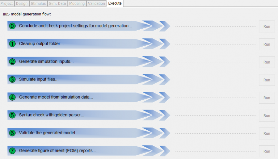
SPISim BPro’s IBIS modeling flow
Let’s talk about these steps in more details.
- Collect: Take this buffer design as an example. If we are going to create an IBIS model for this buffer, first we need to obtain the original spice net list which mostly contains many transistors. Besides, we also need to know under which condition this buffer is manufactured. That means we will need manufacturing process info. We also need to know its nominal operation condition, i.e. voltage supply. Lastly, we need to know at what temperature this buffer is expected to be operated at… as transistor’s performance is affected by the temperature quite a bit. Together, these are usually called P/V/T corners (Process, Voltage, Temperature). Lastly, we need to know what each of the buffer terminals should connect to (bias condition) in order to operate. Normally, a buffer will have many control “legs” which circuit designers can use to fine tune its performance such as slew rate and output impedance. Different settings for control legs will yield buffer with different performance. As an IBIS modeling engineer, you will need to obtains the settings, usually are series of bits flags, for these control legs. With all these information ready, you then can create schematic net list to excite the buffer for modeling.

Transistor and process info. for a buffer design
- Generate: In this step, one needs to excite buffer in order to extract simulation data for different IV/VT/IT tables. Different buffer model type requires different tables. The following give simple overview of how buffer needs to behave for different table’s extractions needs:
- IV for PU: enable the buffer to output high state, sweep voltage at output pad from -Vcc to 2Vcc to get input current;
- IV for PD: enable the buffer to output low state, sweep voltage at output pad from -Vcc to 2Vcc to get input current;
- IV for PC: put it in high Z state while provide input to like it will output high state, sweep voltage at output pad from -Vcc to 2Vcc to get input current;
- IV for GC: put it in high Z state while provide input to like it will output low state, sweep voltage at output pad from -Vcc to 2Vcc to get input current;
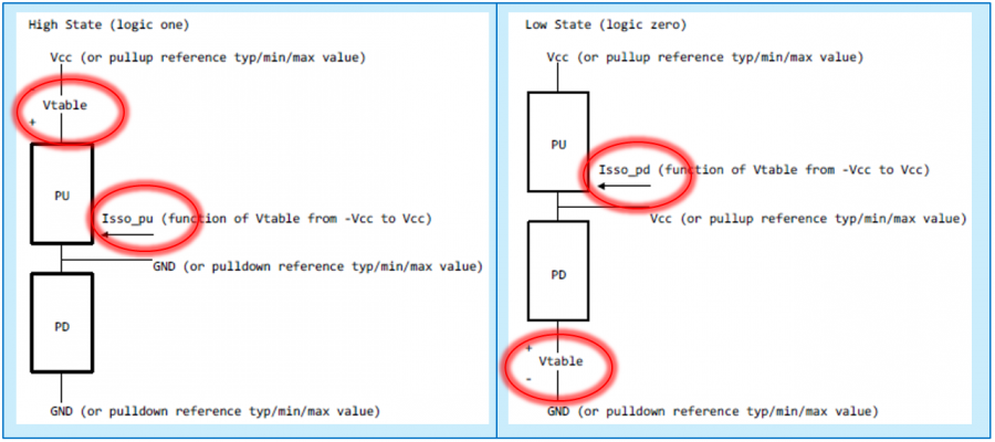
- ISSO PU: put a variable voltage source between ideal supply voltage and buffer’s pull-up terminals, then measure input current at output pad while the voltage sweep from -Vcc to Vcc. This mimics buffer operating under non-ideal voltage supply condition (i.e. voltage droop).
- ISSO PD: put a variable voltage source between ideal ground and buffer’s pull-down terminals, then measure input current at output pad while the voltage sweep from -Vcc to Vcc. This mimics buffer operating under non-ideal grounding condition (i.e. ground bounce).
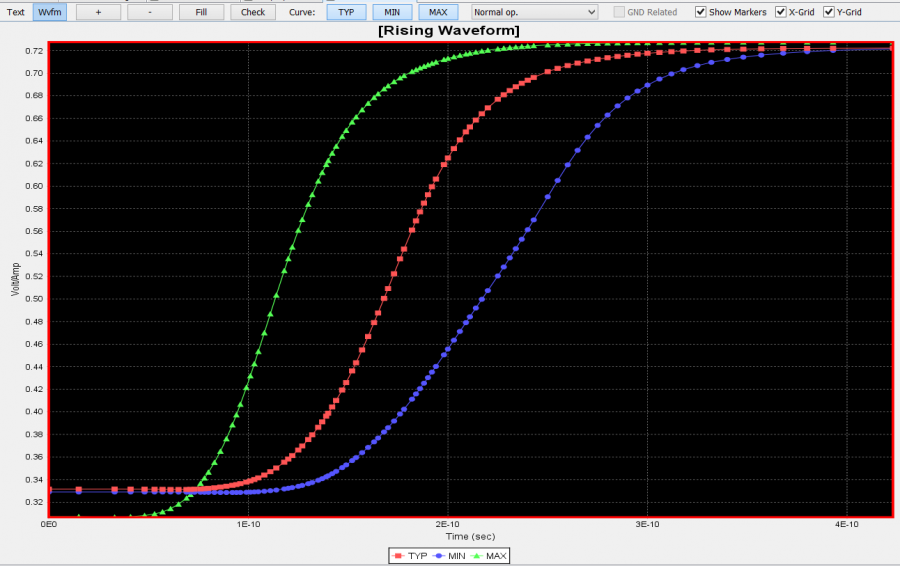
- VT for rising/falling waveform: Connect buffer’s output to test loads and make buffer operate for low to high and high to low transition. Note that the input stimulus’s ramp rate should be practical (e.g. 100ps) as there is no instantaneous logic transition in real world. Do this again for different test loads. At least two VT simulation should be performed, with these two test loading conditions cover the actual usage range of the generated buffer.
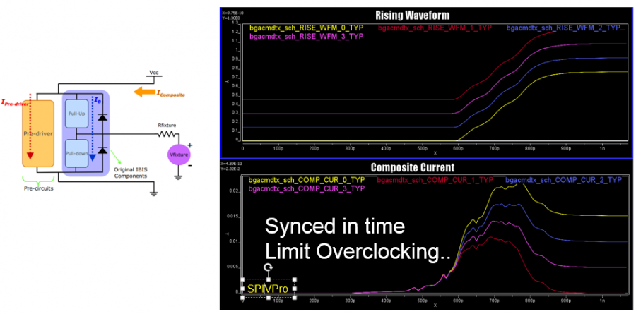
- IT for composite current: Put a zero-volt voltage source between ideal voltage source and buffer’s pull-up circuitry. Monitor its drawing current as buffer runs during operations for previous VT simulation. Typically IT and VT set-up can be combined in one simulation;
- Simulate: The aforementioned net lists file can be generated either separately, i.e. one net list targeted for one IV/IT/VT table extractions, or be combined in one single deck and simulate sequentially using like HSpice’s “.alter” statement. The advantage of doing it separately is that these netlist can be simulated in parallel either using different threads on the same machine or using simulation farm/pool. One might need to perform “pseudo transient” simulation instead of true DC sweep as either some of the buffer design has clock signal or they tends to have convergence issue when doing pure DC sweep.
BPro generated netlist files
- Calculate: In this step, the simulation results need to be visually inspected first to make sure the buffer outputs are desired. If not, one needs to go back to the first step and see whether there are missing bias condition needed to apply to buffer or the simulation setup is incorrect. Remember… garbage in, garbage out! If the simulation waveform is as expected, then the calculation step usually involve subtracting the always existed PC/GC reverse bias current portion from IV data for PU and PD, and switch the voltage for PC and PU such that they will be Vcc relative. If there is on die termination, the PC/GC current will be significant and may needs other special treatment. [Linked to Bob Ross’s paper]
- Model: This step involves translating the calculated data table, along with its operation and loading conditions when the buffer is simulated, into IBIS syntax compatible format. To make data table compact and accurate, an optimization process is usually needed such that best 100 or 1000 points of data are selected from the sometime lengthy time-domain simulation results. Also, all Typ/Min/Max waveform columns have same time point at particular time. so the optimization process needs to take these into account. This optimization process is important for IBIS V3.2 model which only allows 100 data points in the table, and IBIS V5.0 model as well as the composite current is usually very “spiky” and best points need to be selected properly in order to capture most of the current behavior.
BPro’s algorithm selects best 100/1000 points
- Check: Once we have generated an IBIS model, the first step of sanity check is to invoke golden parser to check the syntax. Besides, it will also detect possible dc mismatch issue which implies the quality problem of the generated model. If the difference is beyond certain percentage, it will be flagged as error by the golden parser and most industry circuit simulator will refuse to run on these models. So it’s crucial to iron out and fix any errors and minimize the warning messages.
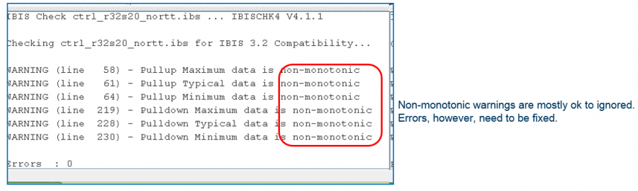
BPro uses golden parser to check syntax and detect errors
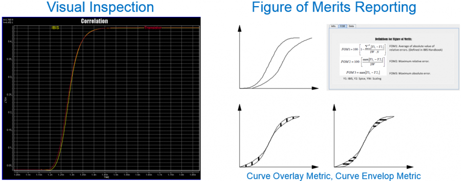
- Validation: Once a syntax valid IBIS model is generated, one needs to further validate its performance and ensure it correlates to the original buffer design well. The validation net list contains instantiated IBIS instance alone with same test loading condition used for original buffer excitation. A good IBIS model is not only accurate, compact, but also run very fast without any convergence issue. So this step should run very fast. One can then visually check and correlate the simulation waveform produced by both original buffer in the “simulation” step and those produced by this just created buffer. Except for the leading delay which IBIS model is not intended to capture, the transition waveform shape and dc steady state should correlate very well.
- Report: A quantitative report is usually expected to demonstrate the quality of the generated buffer. IBIS accuracy handbook and quality spec give spec. on these as industry standard. A “figure of merits” (FOM) is usually used to represent how well the generated IBIS model correlate to original buffer design.
BPro’s visual inspection and FOM reporting
The above is a brief overview of the eight-step IBIS modeling process. There are many details which worth further discussion but are beyond the scope of this post. As one can see, there are many steps involved. While creating IBIS model manually is possible, yet it’s time consuming and error prone. That is why we SPISim developed the BPro module to address the needs for the streamlined modeling process.