In the past, we have blogged several articles regarding buffer modeling. The flow and focus there are mainly for single-ended. The considerations are that:
- Single ended (SE) buffer modeling is a good introduction to modeling flow in general without further complication;
- (Pseudo) differential buffer can actually be modeled as two single-ended buffers;
- Many (true/half) differential buffer can be modeled like pseudo differential buffer without significant loss of accuracy [LINK]
- Differential buffer modeling involve several steps which are a little more complicated.
During our workshops in Taiwan last month, several attendees asked about CML (current-mode logic) modeling. With the maturing of the concepts in SE modeling and the prevalence of SERDES interfaces such as USB, SATA, PCIe etc, we think it’s a good time to revisit the differential modeling flow in more details. We will also show how this design concepts are realized in our SPIBPro in next post.
Note that the contents of this and next posts are also written in conjunction with the paper submission to the IBIS summit later this year.
Model descriptions:
[The info. here are summarized from the IBIS cookbook V4]
A differential buffer can be categorized into three different types:
- Pseudo differential: shown in the rightmost of the picture below. The “P” and “N” driving portion are mutually independent. There is no coupling between these two pins in the circuit.
- Half differential: shown in the middle. the pull-down portion of the “P” and “N” are coupled via a current source or shared load.
- True differential: shown in the leftmost. Both the pull-up and pull-down circuits are coupled via “current-mirror” and shared current source.

For pseudo differential type buffer, the single ended buffer modeling flow can be applied directly. One only needs to generate these two “uncoupled” buffer separately (or use the same model with input flipped) and describe their differential behavior using the “diff pin” IBIS keyword:

Note that this “Diff Pin” keyword is also optional. So one may also simply instantiates two instance of the single ended buffer and use them together outside the IBIS file, such as in the spice netlist.
True/half differential buffer:
For a true/half differential buffers, the existence of “coupling” between P and N circuits must be described using existing IBIS syntax. There are two ways to do so: either using “series” or “external model” keywords:
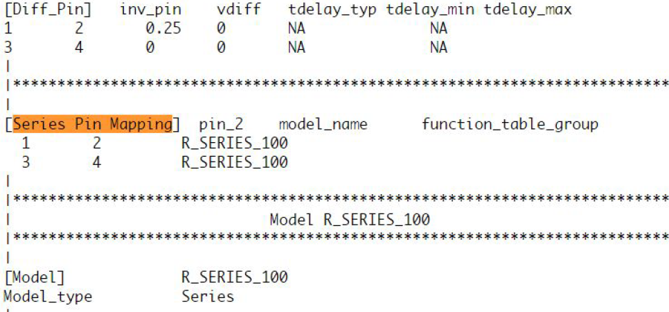
- Series: There are two places series needs to be declared: the first one is “[series pin mapping]” in the model headers and the other one is “series model” of the “coupling” circuit in the “[model]” descriptions:
 Take the picture shown above as an example. Under the “Series Pin Mapping” keyword, a model named “R_SERIES_100” is declared to connect pin 1 to and 2. Another instance of such model also sit between pin 3 and 4. Pin 1~4 each has its own model defined in other part of the ibis file already. For example, pin 1, 2 may have an output buffer connected while pin 3, 4 have open-drain buffers. This R_SERIES_100 model must have type “Series” defined as part of the IBIS file. Since “Series” is one of predefined IBIS model type, its contents (keywords) are not free form and must be one or more of the following series elements: R, L, C, Series current and Series MOSFET which contains up to 100 I/V tables under different biasing voltages.
- External Model: In the IBIS spec, four different differential specific model types are also support.:
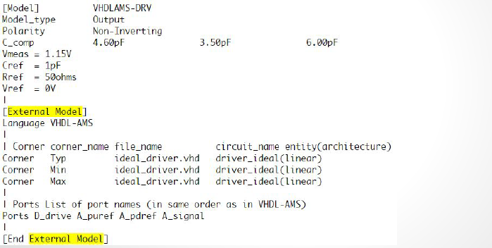
 These differential model types must be implemented with language such as Spice, VHDL-AMS, Verlog-AMS, IBIS Interconnect Spice Sub-circuits (IBIS ISS) and declared with the “External” model section. These languages provides much more flexibility in terms of modeling capabilities, yet they also diminish the portability of the generated IBIS model.
 In the example above, a separate file “ideal_driver.vhd” must be provided outside the IBIS file and an “entity” of name “driver_ideal” needs to be defined. The port connections is described using reserved keywords after the “Ports” statement. In the IBIS Spec, all possible ports are pre-defined and the declaring order here must match their definitions in the associated Verilog/VHDL etc file.
Modeling process:
Pure method 2 implementation, i.e. coding in language like Verilog/VHDL, is up to the model developer. On the other hand, the syntax and structure of series elements, used in method 1, is strictly limited. Thus the modeling process below focuses on method 1 above, i.e. the series model method.
As the coupled half/true buffer described by separated single drivers and connected via a series model for the coupling, the modeling flow must somehow be able to extract the data for these blocks independently so that they can be described with conformed IBIS keyword and reproduce the response when putting together.
For the “Driver” block, it’s a generic input/output/IO type buffer. So tables such as pull-up/pull-down/power-clamp/ground-clamp, when applicable, must be extracted. So are the transient waveform under different test loads. The extraction must be done such that the coupling with other half can be separately as an independent “series element” model.
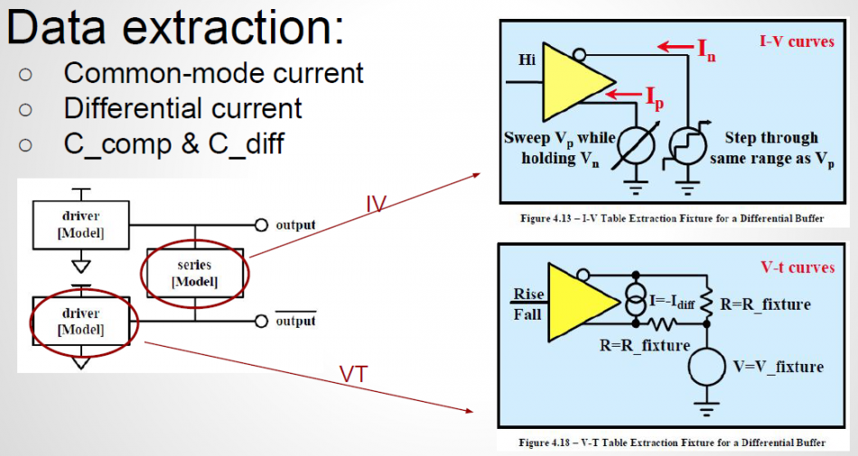
- PU/PD: A two dimensional table produced by sweeping at both the P and N outputs are performed, as shown in the upper right block above. One major assumption for PU/PD extraction is that when both output pins are at the same voltage level, there will be no current flowing through the series model (i.e. the coupling portion). So in that condition, we can assume the series model does not exist at all. The current flows into or out of the buffer at that point is considered as “common-mode” current. This common-mode info is than extracted from surface table and modeled as pull-up and pull-down IV. The whole surface is then shifted vertically by subtracting this common-mode current at every x/y grids. The resulting surface table is considered as the differential current (resistance portion of the series model) and will affect the output when voltage at N and P are different. Note that to satisfy the aforementioned assumption of zero current through series element at common mode voltages, the sweep done at the P/N pins must step very slowly such that the charging/discharging of the reactive components, such as C_Comp or C_Diff can be neglected.
- PC/GC: Clamp table in IBIS are always optional. On the other hand, when a circuit have current which always exist and can’t be turned-off, these data must go to PC/GC to avoid being double counted. That is, the PC/GC table must account for current which always exist and this current will be subtracted from the PU/PD table during the modeling process to avoid being double counted. Situations like this include the ESD circuitry and/or pull-up portion of the half-differential buffer. For PC/GC extraction, common mode sweep like that for PU/PD needs to be performed while buffer is disabled (put into high-Z state). The common mode current will then be extracted as the PC/GC table. Differential mode current is disregarded as it has been accounted for in the PU/PD differential data.

- C_Comp/C_Diff: An important step here is to extract and compute the differential capacitance, C_Diff. This has to be done before VT simulation. It is because C_Diff will affect the transient state differential current, thus it must be accounted for before VT transient simulation. The extracted value will be part of the series element model by adding as C_series. In real design, the C_Comp and C_Diff are both frequency and voltage dependent. So an user can perform 2D sweep in these two dimensions and select a proper value for C_Diff. This formula to calculate c_diff/c_comp is shown above.
- VT waveform: With both static (resistive) data being processed from PU/PD/PC/GC simulation, and the reactive data, i.e. C_Diff, computed from the C_Die simulation. these two info can then be modeled together to be eliminated during VT simulation. The considerations is that: once the effect of coupling part is removed, then the remaining data can be considered as single ended and model accordingly. Having that said, reader should realize that there are much more details involved in this step. For example, how do you model these data? Two approaches may be considered:
- Use E/F/G/H control element: the surface data can be fit to minimize the mean squared error. Resulting coefficients are then realized using poly function or like of a control sources.
- Create a series element: decide the proper components and then create a series element.
Interested user may find some study presented in IBIS summit, such as [this one]
As one can see, the modeling process for a differential buffer is not linear and a certain order must be followed. Inaccurate common-mode extraction will affect IV tables and cause dc-mismatch of the steady state. In addition, failure to extract C_Diff and model different current accurately will greatly impact the accuracy of the transient data. We will see how a modeling flow should take these into account and be validated easily. These are also design concepts behind our SPIBPro flow.

